Agentic AI accelerates 3D IC engineering for the AI factory era
By Sudarshan Deo, software R&D Manager for 3D IC, Siemens
What if you could completely rethink what an EDA workflow looks like for the increasingly complex 3D ICs powering the next generation of AI factories? Siemens’ expanded agentic AI portfolio is automating the hardest parts of 3D IC engineering.
차세대 AI 팩토리를 구동하는 점점 더 복잡해지는 3D IC를 위해 EDA 워크플로우의 개념을 완전히 다시 생각할 수 있다면 어떨까요? 지멘스의 확장된 에이전틱(Agentic) AI 포트폴리오는 3D IC 엔지니어링의 가장 어려운 부분들을 자동화하고 있습니다.
At NVIDIA GTC Berlin 2026, Siemens announced an expansion of its EDA agentic AI portfolio, developed in collaboration with NVIDIA. The announcement represents a significant step forward in applying AI-driven automation to one of the semiconductor industry’s most complex challenges: designing advanced 3D IC systems for the next generation of AI computing.
지멘스는 NVIDIA GTC 베를린 2026에서 NVIDIA와 협력하여 개발한 EDA 에이전틱 AI 포트폴리오의 확장을 발표했습니다. 이번 발표는 차세대 AI 컴퓨팅을 위한 첨단 3D IC 시스템 설계라는 반도체 산업의 가장 복잡한 난제 중 하나에 AI 기반 자동화를 적용하는 데 있어 중요한 도약을 의미합니다.
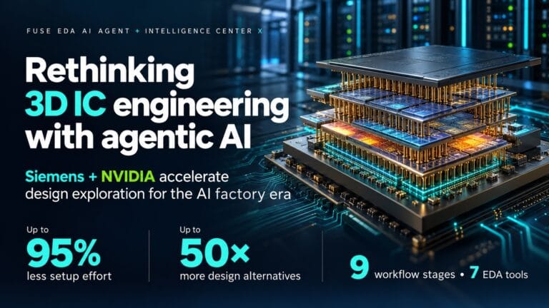
At the center of this innovation is the Fuse EDA AI Agent, integrated with Intelligence Center X. Together, they orchestrate nine automated workflow stages across seven Siemens electronic design automation (EDA) tools, reducing setup effort by up to 95 percent. This automation enables engineering teams to evaluate up to 50 times more design alternatives, helping them address increasingly difficult power and thermal constraints in advanced 3D IC packages.
이 혁신의 중심에는 인텔리전스 센터 X(Intelligence Center X)와 통합된 퓨즈 EDA AI 에이전트(Fuse EDA AI Agent)가 있습니다. 두 시스템은 지멘스의 7개 전자 설계 자동화(EDA) 툴에 걸쳐 9가지 자동화된 워크플로우 단계를 조율하여 설정 노력을 최대 95%까지 줄여줍니다. 이러한 자동화를 통해 엔지니어링 팀은 최대 50배 더 많은 설계 대안을 평가할 수 있으며, 첨단 3D IC 패키지에서 점점 더 까다로워지는 전력 및 발열 제약 조건을 해결하는 데 도움을 받을 수 있습니다.
AI Factories Are Redefining Chip Design Requirements
AI factories are reshaping semiconductor requirements. As AI workloads grow in scale and complexity, the silicon powering these systems must deliver greater compute performance and memory bandwidth while improving thermal efficiency—all within increasingly constrained physical footprints.
AI 팩토리는 반도체 요구 사항을 재편하고 있습니다. AI 워크로드의 규모와 복잡성이 커짐에 따라, 이러한 시스템을 구동하는 실리콘은 더 엄격해진 물리적 공간 제약 속에서도 향상된 전력 효율성을 동시에 확보하면서 더 높은 연산 성능과 메모리 대역폭을 제공해야 합니다.
As compute and memory are brought closer together in tightly integrated 3D packages, power density rises and heat becomes more concentrated. Thermal behavior can no longer be addressed late in the design cycle; electrothermal co-design must be a primary consideration from the earliest stages of development.
긴밀하게 통합된 3D 패키지 안에서 연산과 메모리가 서로 가까워짐에 따라 전력 밀도가 높아지고 열이 더 집중됩니다. 발열 거동은 더 이상 설계 주기의 후반부에 다루어질 수 없으며, 전기·열 공동 설계(electrothermal co-design)는 개발 초기 단계부터 최우선으로 고려되어야 합니다.
The Growing Challenge of Engineering Complexity
Designing these advanced systems presents a major challenge for engineering teams.
이러한 첨단 시스템을 설계하는 것은 엔지니어링 팀에게 큰 도전 과제입니다.
Today, addressing power, thermal, and performance requirements often requires specialists to manually coordinate workflows across multiple tools and design domains. Engineers must continuously move data between electrical, power, thermal, and extraction analyses while repeatedly iterating to achieve design goals.
오늘날 전력, 발열, 성능 요구 사항을 충족하려면 전문가들이 여러 툴과 설계 도메인에 걸쳐 수동으로 워크플로우를 조율해야 하는 경우가 많습니다. 엔지니어들은 설계 목표를 달성하기 위해 반복적으로 반복 작업을 수행하면서 전기, 전력, 열, 추출(extraction) 분석 간에 데이터를 지속적으로 이동시켜야 합니다.
As 3D IC architectures integrate more chiplets, interconnects, power-delivery networks, and thermal interfaces within a tightly constrained package, the number of interacting design variables grows significantly. Time and compute limitations can restrict how many of these coupled scenarios engineering teams evaluate, allowing power, thermal, or performance bottlenecks to remain hidden until late in the design process, when changes are more costly and difficult to implement.
3D IC 아키텍처가 촘촘하게 제약된 패키지 내부에 더 많은 칩렛, 상호 연결(interconnect), 전력 공급 네트워크, 열 인터페이스를 통합함에 따라 상호 작용하는 설계 변수의 수가 크게 증가합니다. 시간 및 연산 능력의 한계로 인해 엔지니어링 팀이 평가할 수 있는 결합 시나리오의 수가 제한될 수 있으며, 이로 인해 변경 비용이 크고 구현하기 어려운 설계 프로세스 후반까지 전력, 열 또는 성능 병목 현상이 숨겨져 있게 됩니다.
To find the best solution with confidence, engineering teams need to analyze far more design alternatives than current workflows allow.
확신을 가지고 최적의 솔루션을 찾기 위해, 엔지니어링 팀은 현재의 워크플로우가 허용하는 것보다 훨씬 더 많은 설계 대안을 분석해야 합니다.
Introducing an Agentic Approach to 3D IC Engineering
Siemens is introducing a new engineering model designed to address this challenge, using the Fuse EDA AI Agent, integrated with Intelligence Center X.
지멘스는 인텔리전스 센터 X와 통합된 퓨즈 EDA AI 에이전트를 활용하여 이 문제를 해결하도록 설계된 새로운 엔지니어링 모델을 도입하고 있습니다.
Engineers begin by defining a design objective: from there, the AI agent coordinates the workflow across multiple Siemens tools, automating the execution of complex multi-domain analyses.
엔지니어는 설계 목표를 정의하는 것으로 시작하며, 그 후 AI 에이전트가 여러 지멘스 툴에 걸쳐 워크플로우를 조율하고 복잡한 멀티 도메인 분석의 실행을 자동화합니다.
The agent runs coupled electrothermal simulations, evaluates results, identifies missed design targets, and helps diagnose root causes. Rather than requiring engineers to manually trace issues across multiple domains, the agent can determine whether performance limitations originate from power delivery challenges, placement decisions, material selections, or an interaction among these factors.
에이전트는 결합된 전기·열 시뮬레이션을 실행하고, 결과를 평가하며, 달성하지 못한 설계 목표를 식별하고, 근본 원인을 진단하는 데 도움을 줍니다. 엔지니어가 여러 도메인에 걸쳐 문제를 수동으로 추적하도록 요구하는 대신, 에이전트는 성능 한계가 전력 공급 문제, 배치 결정, 재료 선택 또는 이러한 요소 간의 상호 작용 중 어디에서 기인하는지 파악할 수 있습니다.
This agent-driven approach allows engineers to focus more on innovation and decision-making while reducing the manual effort typically required to manage complex workflows.
이러한 에이전트 기반 접근 방식을 통해 엔지니어들은 복잡한 워크플로우를 관리하는 데 통상적으로 소요되는 수동 노력을 줄이면서 혁신과 의사결정에 더 집중할 수 있습니다.
Accelerating Exploration with NVIDIA AI Technologies
To support these advanced engineering workflows, Siemens leverages NVIDIA Agent Toolkit alongside NVIDIA accelerated computing platforms and CUDA-X libraries.
이러한 첨단 엔지니어링 워크플로우를 지원하기 위해 지멘스는 NVIDIA 가속 컴퓨팅 플랫폼 및 CUDA-X 라이브러리와 함께 NVIDIA 에이전트 툴킷(NVIDIA Agent Toolkit)을 활용합니다.
This combination enables an AI-driven workflow where accelerated simulation tools provide faster results for the agent to evaluate. By shortening simulation turnaround times, engineers can explore substantially more design possibilities within the same project schedule.
이 조합을 통해 가속화된 시뮬레이션 툴이 에이전트가 평가할 수 있는 더 빠른 결과를 제공하는 AI 기반 워크플로우가 가능해집니다. 시뮬레이션 소요 시간을 단축함으로써 엔지니어는 동일한 프로젝트 일정 내에 실질적으로 더 많은 설계 가능성을 탐색할 수 있습니다.
The ability to analyze a far greater number of alternatives is particularly important in advanced 3D IC design, where optimal solutions often emerge only after evaluating numerous trade-offs between performance, power efficiency, thermal behavior, package architecture, and material choices.
훨씬 더 많은 대안을 분석할 수 있는 능력은 첨단 3D IC 설계에서 특히 중요한데, 이 분야에서는 성능, 전력 효율성, 발열 거동, 패키지 아키텍처, 소재 선택 간의 수많은 절충안을 평가한 후에야 비로소 최적의 솔루션이 도출되는 경우가 많기 때문입니다.
From Automation to Engineering Intelligence
Traditional workflows that rely on extensive manual coordination cannot keep pace with the increasing complexity of advanced 3D IC architectures.
광범위한 수동 조율에 의존하는 전통적인 워크플로우는 첨단 3D IC 아키텍처의 증가하는 복잡성을 따라잡을 수 없습니다.
By combining Siemens’ EDA expertise with NVIDIA’s AI and accelerated computing technologies, the Fuse EDA AI Agent and Intelligence Center X introduce a new approach to engineering. Rather than simply automating individual tasks, they enable an intelligent, agent-driven workflow capable of orchestrating analyses, diagnosing design challenges, and expanding design exploration at greater scale.
지멘스의 EDA 전문성과 NVIDIA의 AI 및 가속 컴퓨팅 기술을 결합함으로써, 퓨즈 EDA AI 에이전트와 인텔리전스 센터 X는 새로운 엔지니어링 접근 방식을 선보입니다. 단순한 개별 작업 자동화를 넘어 분석 조율, 설계 과제 진단, 더 큰 규모의 설계 탐색 확장 능력을 갖춘 지능적이고 에이전트 기반의 워크플로우를 구현합니다.
The result is a faster path to optimized designs, allowing engineering teams to address the power and thermal challenges of next-generation AI systems while accelerating innovation for the AI factory era.
그 결과 최적화된 설계로 향하는 더 빠른 경로가 열리며, 엔지니어링 팀은 차세대 AI 시스템의 전력 및 열 문제를 해결하는 동시에 AI 팩토리 시대를 위한 혁신을 가속화할 수 있습니다.
See how Siemens is advancing agentic AI for 3D IC engineering, learn more here: Siemens expands agentic AI to tackle 3D IC thermal | Siemens
지멘스가 3D IC 엔지니어링을 위해 에이전틱 AI를 어떻게 발전시키고 있는지 확인해 보세요. 자세한 내용은 여기에서 확인할 수 있습니다: [지멘스, 3D IC 발열 해결을 위해 에이전틱 AI 확장 | 지멘스]
Sudarshan Deo is a Software R&D Manager for 3D IC at Siemens in the Central Engineering Solutions Division. He holds an M.S. in Computer Science from California State University, Sacramento, and has expertise in implementing and integrating complex 3D IC workflows, including physical design, DFT, multi-physics, thermal, stress, SI, PI, and DC IR-drop analysis. He also contributes to initiatives in 3D UI and data management using IP lifecycle management and integrates advanced AI frameworks to optimize and enhance 3D IC workflows. He serves as a technical point of contact for divisions across Siemens Digital Industries Software.
수다르샨 데오(Sudarshan Deo)는 지멘스 디지털 인스트리즈 소프트웨어(Siemens Digital Industries Software) 중앙 엔지니어링 솔루션 사업부(Central Engineering Solutions Division)의 3D IC 소프트웨어 R&D 매니저입니다. 캘리포니아 주립대학교 새크라멘토(California State University, Sacramento)에서 컴퓨터과학 석사 학위를 취득했으며, 물리적 설계, DFT, 멀티피직스(다물리), 열, 응력, SI, PI, DC IR-드롭 분석을 포함한 복잡한 3D IC 워크플로우 구현 및 통합 분야의 전문성을 가지고 있습니다. 또한 IP 라이프사이클 관리를 활용한 3D UI 및 데이터 관리 이니셔티브에 기여하고 있으며, 3D IC 워크플로우를 최적화하고 향상시키기 위해 첨단 AI 프레임워크를 통합하고 있습니다. 지멘스 디지털 인스트리즈 소프트웨어 내 여러 사업부의 기술적 연락 담당자(PoC) 역할을 맡고 있습니다.



