CEO Interview with Vera Yang of Flexcompute
Source: https://semiwiki.com/ceo-interviews/375564-ceo-interview-with-vera-yang-of-flexcompute/
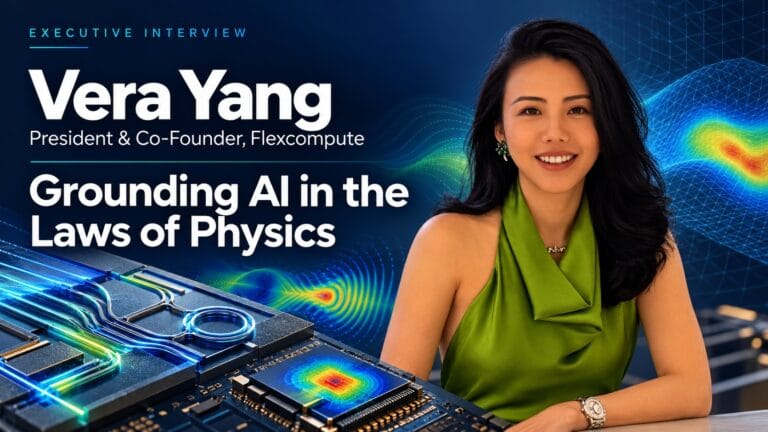
Vera Yang is President and Co-Founder of Flexcompute, a frontier AI lab building a Physics World Model that bridges data-driven AI and the laws of physics. She focuses on the problems where the stakes are highest and the physics hardest, including photonic chips for AI data centers, advanced semiconductor packaging and spacecraft operations in orbit. Before Flexcompute, Vera was a partner at Hedosophia and Warburg Pincus and led the New York Stock Exchange’s Asia business, advising more than 30 companies.
베라 양(Vera Yang)은 데이터 기반 AI와 물리학 법칙을 연결하는 피직스 월드 모델(Physics World Model)을 구축하는 최첨단 AI 랩인 플렉스컴퓨트(Flexcompute)의 공동 창립자이자 대표(President)입니다. 그녀는 AI 데이터센터용 광자 칩, 차세대 반도체 패키징, 궤도 상 우주선 운용 등 리스크가 가장 크고 물리학적 난도가 높은 문제들에 집중하고 있습니다. 플렉스컴퓨트에 합류하기 전에는 헤도소피아(Hedosophia)와 워버그핀커스(Warburg Pincus)의 파트너였으며, 뉴욕증권거래소(NYSE)의 아시아 사업을 이끌며 30개 이상의 기업에 자문을 제공했습니다.
Tell us about your company?
Flexcompute is a frontier AI lab building a Physics World Model, which grounds AI in the laws of physics so engineers and AI agents can know how a design will perform before it’s built. Researchers from Stanford and MIT founded the company, and our team of more than 70 PhDs builds physics solvers for electromagnetics, fluid dynamics, structures and heat. Through Tokenized Physics, we build neural networks and our physics solvers directly into one model. It represents complex physical systems efficiently while preserving the governing physics, which makes our validated solvers fast enough to work inside AI-driven design loops and gives AI a verification layer grounded in trusted physics.
Flexcompute는 엔지니어와 AI 에이전트가 제품을 실제로 제작하기 전에 설계 성능을 미리 파악할 수 있도록, AI에 물리학 법칙을 접목하는 피직스 월드 모델을 구축하는 최첨단 AI 랩입니다. 스탠퍼드와 MIT 출신 연구원들이 회사를 설립했으며, 70명이 넘는 박사들로 구성된 저희 팀은 전자기학, 유체역학, 구조역학, 열역학 분야의 물리 솔버(solver)를 개발하고 있습니다. 저희는 토크나이즈드 피직스(Tokenized Physics)를 통해 신경망과 물리 솔버를 단일 모델로 통합합니다. 이를 통해 지배 방정식을 충실히 보존하면서 복잡한 물리 시스템을 효율적으로 표현할 수 있으며, 검증된 솔버를 AI 기반 설계 루프 내부에서 구동될 수 있을 만큼 빠른 속도로 구현하고, 신뢰할 수 있는 물리학 기반의 검증 계층을 AI에 제공합니다.
More than 250 companies use our technology across semiconductors, photonics, aerospace, automotive and defense. SemiWiki readers may know us through Tidy3D, our photonics and electromagnetics solver, and PhotonForge, our photonic chip design platform. In October, Samsung Ventures and Applied Ventures invested in Flexcompute.
반도체, 포토닉스, 항공우주, 자동차, 국방 분야에 걸쳐 250개 이상의 기업이 당사 기술을 사용하고 있습니다. SemiWiki 독자분들이라면 광자학 및 전자기학 솔버인 Tidy3D와 광칩 설계 플랫폼인 PhotonForge를 통해 저희를 잘 알고 계실 것입니다. 지난 10월에는 삼성벤처투자(Samsung Ventures)와 어플라이드벤처스(Applied Ventures)가 Flexcompute에 투자했습니다.
What problems are you solving?
AI needs more chips, and the way to design more of them better is with AI agents working alongside engineers. Agents are already good at generating designs. Our team asked a group of five agents to rebuild photonic circuits from published papers, and they have built 34 so far, including a 32×32 switch with 1,024 Mach-Zehnder interferometers. Every one passed DRC and LVS.
AI에는 더 많은 칩이 필요하며, 더 많은 칩을 더 훌륭하게 설계하는 방법은 엔지니어와 함께 일하는 AI 에이전트를 활용하는 것입니다. 에이전트는 이미 설계를 생성하는 데 뛰어납니다. 저희 팀은 5개의 에이전트로 구성된 그룹에게 공개된 논문에서 광회로를 다시 구축하도록 요청했고, 현재까지 1,024개의 마흐-젠더 간섭계(Mach-Zehnder interferometer)를 갖춘 32×32 스위치를 포함해 34개를 구축했습니다. 모든 제품이 DRC(설계 규칙 검증)와 LVS(레이아웃 대 회로 검증)를 통과했습니다.
So the hard part is shifting from generating options to knowing which ones will work: capturing design intent, simulating the full circuit and closing the loop with measured data. That is the problem we solve. Flexcompute validates every design against real-world physics at the speed of AI, giving engineers the freedom to explore and the confidence to build.
따라서 어려운 부분은 단순히 옵션을 생성하는 단계에서 '어떤 것이 실제로 작동할지 파악하는 단계'로 전환하는 것입니다. 즉, 설계 의도를 포착하고, 전체 회로를 시뮬레이션하며, 측정된 데이터와 피드백 루프를 완성하는 것입니다. 이것이 바로 저희가 해결하는 문제입니다. Flexcompute는 AI의 속도로 실제 물리 법칙에 기반하여 모든 설계를 검증함으로써, 엔지니어에게는 탐구의 자유를, 빌더에게는 확신을 제공합니다.
What application areas are your strongest?
Photonics is our deepest. Teams at AMD, Anduril, Nvidia, Samsung Display, Coherent, TDK, Ayar Labs, and Global Foundry use our solutions to integrate foundry PDKs and EDA tools. Optical I/O and co-packaged optics for AI data centers are the fastest-growing part of that work.
포토닉스 분야에서 가장 깊이 있는 전문성을 가지고 있습니다. AMD, 안두릴(Anduril), 엔비디아(Nvidia), 삼성디스플레이(Samsung Display), 코히어런트(Coherent), TDK, 에이어 랩스(Ayar Labs), 글로벌파운드리(GlobalFoundries)의 팀들이 파운드리 PDK 및 EDA 툴을 통합하기 위해 당사 솔루션을 사용하고 있습니다. AI 데이터센터를 위한 광 인터커넥트(Optical I/O)와 동반 패키징 광학(Co-packaged optics) 분야는 이 작업 중 가장 빠르게 성장하는 영역입니다.
We’re also strong in the physics of advanced packaging: heat, stress, warpage and reliability. As chiplets, HBM and optics share one package, those effects interact. Tokenized Physics lets engineers ask system-level questions that used to be too large or too slow to simulate. Our warpage Physics Twin, for example, predicts which of more than 800,000 solder points will fail under heat before the design goes to production.
또한 어드밴스드 패키징(고성능 패키징)의 물리학, 즉 열, 응력, 휨(warpage), 신뢰성 분야에서도 강점을 보입니다. 칩렛(chiplet), HBM, 광학이 하나의 패키지를 공유할 때 이러한 영향들은 상호 작용합니다. 토크나이즈드 피직스를 통해 엔지니어들은 기존에는 시뮬레이션하기에 너무 거대하거나 느렸던 시스템 수준의 질문들을 던질 수 있습니다. 예를 들어, 당사의 휨(warpage) 피직스 트윈(Physics Twin)은 디자인이 생산에 들어가기 전에 80만 개가 넘는 솔더 포인트 중 어느 부분에 열로 인한 결함이 발생할지 예측합니다.
What keeps your customers up at night?
Respins. A photonic chip or advanced package that fails after tapeout costs months and millions of dollars, and the stakes rise as optics move closer to the processor. The most dangerous problems hide between components. One of our engineers recently built a full optical I/O chip in PhotonForge, eight wavelength channels at 100 Gb/s each, in an agentic workflow. Each demultiplexer filter had about −18 dB of crosstalk to its neighbor, which looks fine on a datasheet. Simulated as a full link with every channel present, the leakage added up across the receiver and noticeably degraded the eye. You only see that when the whole chip is simulated together.
리스핀(Respins) 문제입니다. 테이프아웃(제조용 도면 전달) 이후에 실패하는 광칩이나 어드밴스드 패키지는 수개월의 시간과 수백만 달러의 비용을 낭비하게 만들며, 광학 기술이 프로세서에 더 가까워질수록 리스크는 더욱 커집니다. 가장 위험한 문제는 컴포넌트 사이에 숨어 있습니다. 최근 저희 엔지니어 중 한 명이 에이전틱 워크플로우를 통해 PhotonForge에서 각각 100 Gb/s 속도의 8개 파장 채널을 가진 완전한 광 인터커넥트 칩을 제작했습니다. 각 디멀티플렉서 필터는 이웃 채널과의 누화(crosstalk)가 약 -18 dB로 데이터시트상에서는 문제가 없어 보였습니다. 하지만 모든 채널이 존재하는 전체 링크로 시뮬레이션해 보니, 누화가 수신단 전체에 걸쳐 누적되어 아이패턴(eye pattern)이 눈에 띄게 저하되었습니다. 이러한 문제는 칩 전체를 함께 시뮬레이션할 때만 확인할 수 있습니다.
And as teams bring agents into the flow, the question becomes: if an agent proposes a design, can we trust it enough to send it to the fab? Our answer is to put trusted physics behind every step.
또한 팀들이 에이전트를 워크플로우에 도입함에 따라 다음과 같은 질문이 대두됩니다. "에이전트가 제안한 설계를 팹(fab)에 보낼 수 있을 만큼 신뢰할 수 있는가?" 저희의 해답은 모든 단계 뒤에 신뢰할 수 있는 물리학을 배치하는 것입니다.
What does the competitive landscape look like and how do you differentiate?
There are established simulation and EDA vendors, and a growing number of AI companies building surrogate models trained on past simulation data. Surrogates are only as good as their data and can be confidently wrong on a design no one has seen before. We differentiate in three ways.
- First, we build our own frontier physics capabilities through novel solvers across multi-physics domains, so answers come from validated physics rather than from patterns in old data.
- Second, Tokenized Physics builds neural networks and first-principles physics into one model, so we can handle multi-scale problems that no other simulation company can solve.
- Third, our verification layer is agent-native and fast enough to keep pace with generative design, checking every design against the laws of physics as quickly as AI can create it.
기존의 시뮬레이션 및 EDA 벤더들이 존재하며, 과거 시뮬레이션 데이터를 학습한 대용(surrogate) 모델을 구축하는 AI 기업들도 늘고 있습니다. 대용 모델은 학습 데이터만큼만 우수하며, 한 번도 본 적 없는 설계에 대해서는 자신 있게 틀린 답을 낼 수 있습니다. 저희는 세 가지 측면에서 차별화됩니다.
- 첫째, 멀티피직스(다물리) 도메인 전반에 걸친 새로운 솔버를 통해 독자적인 최첨단 물리학 역량을 구축하므로, 과거 데이터의 패턴이 아닌 검증된 물리학을 기반으로 해답을 도출합니다.
- 둘째, 토크나이즈드 피직스는 신경망과 제1원리 물리학을 단일 모델로 통합하여, 다른 어떤 시뮬레이션 기업도 해결할 수 없는 다중 스케일(multi-scale) 문제를 처리할 수 있습니다.
- 셋째, 당사의 검증 계층은 에이전트 네이티브이며 제너러티브(Generative) 설계의 속도에 발맞출 수 있을 만큼 빠릅니다. AI가 생성하는 것만큼 빠른 속도로 물리 법칙에 따라 모든 설계를 확인합니다.
What new features/technology are you working on?
In October we released PhotonForge 2.0, built on a simple idea: agents will increasingly design chips with engineers, so both need the same tools. Engineers and agents work on one design, from PDK and schematic through layout, multi-physics simulation, DRC, LVS and tapeout. Recent releases added physics-verified compact models and automatic Verilog-A export, so device physics carries through to circuit simulation.
지난 10월, 저희는 "에이전트가 엔지니어와 함께 점점 더 많은 칩을 설계할 것이므로 둘 다 동일한 툴을 필요로 할 것"이라는 단순한 아이디어를 바탕으로 구축된 PhotonForge 2.0을 출시했습니다. 엔지니어와 에이전트는 PDK 및 회로도부터 레이아웃, 멀티피직스 시뮬레이션, DRC, LVS, 테이프아웃에 이르기까지 하나의 설계에서 함께 협업합니다. 최근 출시 버전에는 물리학 검증이 완료된 콤팩트 모델과 자동 Verilog-A 내보내기 기능이 추가되어, 소자 물리학이 회로 시뮬레이션까지 이어지도록 지원합니다.
Next, we’re extending physics verification of AI-assisted designs into the industry-standard EDA flows our customers rely on, and expanding our Physics Twins for advanced packaging, starting with warpage, thermal, and signal integrity problems. All of them are proven by Flexcompute’s Physics World Model.
다음으로, 고객이 의존하는 산업 표준 EDA 플로우로 AI 보조 설계의 물리 검증 범위를 확장하고 있으며, 휨, 열, 신호 무결성 문제를 시작으로 어드밴스드 패키징용 피직스 트윈을 확장하고 있습니다. 이 모든 것은 Flexcompute의 피직스 월드 모델을 통해 입증됩니다.
How do customers normally engage with your company?
Most teams start with PhotonForge Community. It’s free, runs on the engineer’s own machine, and any agent can start using it from our docs. When a team is ready to take designs to production, Enterprise adds foundry PDK integration, EDA connectors, version control and traceability that ties every revision to the tapeout and to the data measured back.
대부분의 팀은 PhotonForge Community 버전으로 시작합니다. 무료이며 엔지니어의 로컬 기기에서 실행되고, 문서화되어 있어 어떤 에이전트든 바로 사용할 수 있습니다. 팀이 설계를 프로덕션 단계로 가져갈 준비가 되면, 엔터프라이즈 버전은 파운드리 PDK 통합, EDA 커넥터, 버전 제어, 그리고 모든 수정 사항을 테이프아웃 및 측정 데이터와 연결하는 추적성을 제공합니다.
For the hardest, highest-stakes problems, like warpage in advanced packages, we work directly with a customer’s team to build a Physics Twin: a working model of their product, backed by our solvers, that their engineers and AI agents can question, test and improve before anything is built. We also run agentic design workshops and complimentary teaching programs for universities.
고급 패키징의 휨 현상처럼 가장 어렵고 리스크가 큰 문제에 대해서는, 고객 팀과 직접 협력하여 피직스 트윈을 구축합니다. 이는 당사의 솔버를 기반으로 하는 고객 제품의 작동 모델로서, 제품이 제작되기 전에 엔지니어와 AI 에이전트가 질문을 던지고, 테스트하며, 개선할 수 있도록 지원합니다. 또한 에이전틱 설계 워크숍과 대학을 위한 무료 교육 프로그램도 운영하고 있습니다.



