CTO Interview with Dr. Zakir Syed of ClockEdge
Source: https://semiwiki.com/eda/clockedge/374633-cto-interview-with-dr-zakir-syed-of-clockedge/
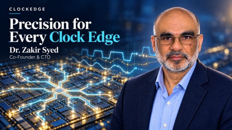
Dr. Zakir Syed is Co-founder and Chief Technology Officer of ClockEdge, where he has played a central role in developing specialized simulation technology for advanced semiconductor clock networks. He brings more than 30 years of experience in electronic design automation and semiconductor verification. He joined Simplex Solutions near its inception in 1995, contributing to technologies addressing timing, power, signal integrity, and reliability.
자키르 사이드(Zakir Syed) 박사는 클록엣지(ClockEdge)의 공동 창립자이자 최고기술책임자(CTO)로, 첨단 반도체 클록 네트워크를 위한 특수 시뮬레이션 기술 개발에 중추적인 역할을 해왔습니다. 그는 전자 설계 자동화(EDA)와 반도체 검증 분야에서 30년 이상의 경험을 보유하고 있습니다. 1995년 설립 초기에 심플렉스 솔루션즈(Simplex Solutions)에 합류하여 타이밍, 전력, 신호 무결성, 신뢰성 관련 기술 개발에 기여했습니다.
Zakir has published numerous technical papers on verification and simulation and presented at industry conferences. He holds a master’s degree in Mechanical Engineering and a PhD in Electrical Engineering, both from Duke University.
자키르 박사는 검증 및 시뮬레이션에 관한 다수의 기술 논문을 집필했으며 업계 콘퍼런스에서 발표를 진행해 왔습니다. 듀크 대학교에서 기계공학 석사 학위와 전기공학 박사 학위를 모두 취득했습니다.
What brought you to ClockEdge?
Earlier in my career at Simplex Solutions, I worked on technologies for analyzing large electrical networks. One of the recurring challenges was maintaining transistor-level accuracy as designs grew increasingly complex.
심플렉스 솔루션즈에서 경력을 쌓던 초기 시절, 저는 대규모 전기 네트워크를 분석하는 기술을 연구했습니다. 반복되는 과제 중 하나는 설계가 점점 더 복잡해짐에 따라 트랜지스터 레벨의 정확도를 유지하는 것이었습니다.
Clock networks were particularly interesting because they are the most critical distribution networks in a synchronous SoC. An SoC has multiple clocks, and together their networks reach every sequential element. In high-performance processors, clock distribution can account for roughly 30% of total chip power.
클록 네트워크는 동기식 SoC에서 가장 중요한 배전 네트워크이기 때문에 특히 흥미로웠습니다. SoC에는 여러 개의 클록이 존재하며, 이들의 네트워크는 모든 순서 논리 소자(sequential element)에 닿습니다. 고성능 프로세서에서 클록 분배는 전체 칩 전력의 약 30%를 차지할 수 있습니다.
Yet even small variations in clock behavior can have significant consequences for performance and reliability. Analyzing the entire network with conventional transistor-level simulation was simply too computationally expensive for practical use on large SoCs.
하지만 클록 거동의 사소한 변조조차도 성능과 신뢰성에 심대한 결과를 초래할 수 있습니다. 기존의 트랜지스터 레벨 시뮬레이션으로 전체 네트워크를 분석하는 것은 대규모 SoC에 실질적으로 적용하기에는 연산 비용이 너무 컸습니다.
We saw an opportunity to develop simulation technology specifically for clocks, combining SPICE-level accuracy with the speed and capacity needed for large designs.
우리는 SPICE 수준의 정확도와 대규모 설계에 필요한 속도 및 용량을 결합하여, 클록만을 위해 특화된 시뮬레이션 기술을 개발할 기회를 보았습니다.
That became the technical foundation of our work at ClockEdge. Today, the opportunity goes beyond accurate analysis to helping engineers use that insight to improve performance, power, and reliability.
그것이 바로 클록엣지에서 수행하는 작업의 기술적 기반이 되었습니다. 오늘날 이러한 기회는 정확한 분석을 넘어, 엔지니어들이 그 통찰력을 활용해 성능, 전력, 신뢰성을 개선할 수 있도록 돕는 데까지 확장되어 있습니다.
What is the biggest challenge your customer is facing?
Our customers are being asked to deliver higher performance with lower power while ensuring their chips operate reliably in silicon. At advanced nodes, that balance is becoming increasingly difficult.
우리 고객들은 칩이 실리콘 상에서 신뢰성 있게 작동하도록 보장하는 동시에, 더 낮은 전력으로 더 높은 성능을 제공해야 한다는 요구를 받고 있습니다. 첨단 노드에서는 이 균형을 맞추기가 점점 더 어려워지고 있습니다.
Timing margins are tighter, and electrical effects that might once have been relatively small can now have a significant impact. Power-supply noise, for example, can shift clock edges and change the relative timing between clock paths. Waveform distortion and duty-cycle changes can further reduce the usable timing window.
타이밍 마진이 더욱 빠듯해졌으며, 한때는 비교적 사소하게 여겨졌던 전기적 효과들도 이제는 상당한 영향을 미칠 수 있습니다. 예를 들어, 전원 공급 노이즈는 클록 에지를 이동시키고 클록 경로 간의 상대적 타이밍을 바꿀 수 있습니다. 파형 왜곡과 듀티 사이클(duty-cycle) 변화는 사용 가능한 타이밍 윈도우를 더욱 축소시킬 수 있습니다.
Engineers compensate for uncertainty by adding timing margin. That is necessary, but excessive margin can come at a substantial cost in frequency, power, or area.
엔지니어들은 불확실성을 보완하기 위해 타이밍 마진을 추가합니다. 이는 필수적이지만, 과도한 마진은 주파수, 전력, 또는 면적 측면에서 상당한 비용을 초래할 수 있습니다.
The difficult question is how much of that margin is actually needed.
어려운 질문은 그 마진 중 실제로 얼마만큼이 필요한가 하는 점입니다.
Customers want to distinguish real electrical risks from conservative assumptions. The better they understand that difference, the more confidently they can pursue aggressive PPA targets without compromising silicon reliability.
고객들은 보수적인 가정과 실제적인 전기적 위험을 구분하고자 합니다. 그 차이를 더 잘 이해할 수록, 칩의 신뢰성을 저해하지 않으면서 더욱 과감한 PPA(전력·성능·면적) 목표를 자신 있게 추구할 수 있습니다.
Why is your approach to solving this problem unique?
We developed simulation technology specifically for clock networks, rather than adapting a general-purpose simulator.
우리는 범용 시뮬레이터를 개조하는 대신, 클록 네트워크만을 위해 특화된 시뮬레이션 기술을 개발했습니다.
By exploiting the characteristics of clock-network topologies, we can analyze complete clock networks, including complex trees and meshes, with SPICE-level electrical accuracy and the speed and capacity needed for large SoCs.
클록 네트워크 토폴로지의 특성을 활용함으로써, 우리는 복잡한 트리와 메시를 포함한 전체 클록 네트워크를 SPICE 수준의 전기적 정확도와 대규모 SoC에 필요한 속도 및 용량으로 분석할 수 있습니다.
Our technology works with industry-standard design data and fits alongside existing implementation and sign-off flows, allowing engineers to introduce detailed electrical analysis without replacing their established tools.
우리의 기술은 업계 표준 설계 데이터와 호환되며 기존 구현 및 사인오프(sign-off) 플로우와 나란히 작동하므로, 엔지니어들은 기존에 구축된 툴을 교체하지 않고도 상세한 전기적 분석을 도입할 수 있습니다.
Our Veridian platform brings together timing, jitter, power, and aging analysis. It allows engineers to examine how electrical effects interact across the network, rather than considering each one in isolation.
당사의 베리디안(Veridian) 플랫폼은 타이밍, 지터, 전력, 그리고 열화(aging) 분석을 하나로 통합합니다. 이를 통해 엔지니어들은 각각의 효과를 개별적으로 보는 대신, 네트워크 전반에서 전기적 효과들이 어떻게 상호작용하는지 검토할 수 있습니다.
But identifying a problem is only part of the job. Engineers also need to know how best to address it.
하지만 문제를 찾아내는 것은 작업의 일부분에 불과합니다. 엔지니어들은 이를 가장 잘 해결하는 방법도 알아야 합니다.
That’s where vHelm comes in. It connects electrical analysis with interactive what-if exploration and Virtual ECOs.
바로 이 지점에서 vHelm이 역할을 합니다. vHelm은 전기적 분석을 대화형 왓이프(what-if) 탐색 및 가상 ECO(Virtual ECOs)와 연결해 줍니다.
Consider resizing a clock buffer to improve timing. That change may also affect power consumption, waveform quality, or jitter elsewhere in the network. With ClockEdge, engineers can examine those trade-offs before committing to a physical design change.
타이밍을 개선하기 위해 클록 버퍼의 크기를 조정하는 상황을 생각해 봅시다. 그 변경은 네트워크의 다른 부분에서 전력 소비, 파형 품질, 또는 지터에도 영향을 미칠 수 있습니다. 클록엣지를 이용하면 엔지니어들은 물리적인 설계 변경에 착수하기 전에 이러한 트레이드오프를 미리 검토할 수 있습니다.
The objective is to make accurate electrical analysis useful for everyday design decisions, not just final verification.
목표는 정확한 전기적 분석을 최종 검증 단계뿐만 아니라 일상적인 설계 결정에도 유용하게 만드는 것입니다.
What other approaches are being used to solve this problem?
Design teams already use sophisticated tools for static timing analysis, power integrity, clock integrity, and circuit simulation. They also rely on statistical methods and guardbanding to manage uncertainty.
설계 팀들은 이미 정적 타이밍 분석(STA), 전력 무결성, 클록 무결성, 그리고 회로 시뮬레이션을 위해 정교한 툴을 사용하고 있습니다. 또한 불확실성을 관리하기 위해 통계적 방법과 가드밴딩(guardbanding)에 의존하고 있습니다.
These approaches serve important purposes, and modern EDA tools can analyze many of the electrical effects we’re discussing.
이러한 접근 방식들은 중요한 목적에 기여하며, 현대 EDA 툴은 우리가 논의하고 있는 많은 전기적 효과들을 분석할 수 있습니다.
The challenge is translating all that information into the best possible clock implementation.
과제는 그 모든 정보를 가능한 최고의 클록 구현으로 번역해내는 것입니다.
A design may meet its timing constraints and still have unnecessary buffering, excess clock power, or more margin than its actual electrical behavior requires. Identifying those opportunities and understanding the consequences of possible changes can involve considerable analysis and iteration.
설계가 타이밍 제약 조건을 충족하더라도 불필요한 버퍼링, 과도한 클록 전력, 또는 실제 전기적 거동이 요구하는 것보다 더 많은 마진을 여전히 가지고 있을 수 있습니다. 그러한 기회를 파악하고 가능한 변경 사항의 결과를 이해하는 것은 상당한 분석과 반복 작업을 수반할 수 있습니다.
This is where we believe ClockEdge offers a valuable approach. By combining full-clock electrical analysis with interactive optimization, engineers can investigate alternatives and evaluate their impact across timing, jitter, power, and aging in one flow.
바로 이 영역에서 클록엣지가 가치 있는 접근 방식을 제공한다고 믿습니다. 전체 클록에 대한 전기적 분석과 대화형 최적화를 결합함으로써, 엔지니어들은 하나의 플로우 안에서 대안들을 조사하고 타이밍, 지터, 전력, 그리고 열화 전반에 걸친 영향을 평가할 수 있습니다.
Meeting timing requirements tells you that a design satisfies its constraints. It doesn’t necessarily tell you whether you’ve achieved the best possible performance and power efficiency.
타이밍 요구사항을 충족한다는 것은 설계가 제약 조건을 만족한다는 것을 의미합니다. 그것이 반드시 가능한 최고의 성능과 전력 효율을 달성했음을 의미하는 것은 아닙니다.
That’s the opportunity we want to help engineers explore.
이것이 바로 우리가 엔지니어들이 탐색하도록 돕고 싶은 기회입니다.
What challenges will your customers face in the near future?
I expect the interaction between transistor behavior, power delivery, and clock performance to become increasingly important.
저는 트랜지스터 거동, 전력 공급, 그리고 클록 성능 간의 상호작용이 점점 더 중요해질 것으로 예상합니다.
The transition to gate-all-around transistors at 2nm and beyond, along with innovations such as backside power delivery, are creating new opportunities for performance and power efficiency. These technologies also change the electrical characteristics and design conditions engineers need to understand.
2nm 이하 공정에서의 게이트 올 어라운드(GAA) 트랜지스터로의 전환은 이면 전력 공급(backside power delivery) 등의 혁신과 함께 성능 및 전력 효율을 위한 새로운 기회를 창출하고 있습니다. 동시에 이러한 기술들은 엔지니어들이 이해해야 하는 전기적 특성과 설계 조건도 변화시키고 있습니다.
At the same time, AI and high-performance computing are driving demanding performance-per-watt requirements. Designs have increasingly complex operating modes, power-management strategies, and workloads that can change electrical conditions dynamically.
동시에 AI와 고성능 컴퓨팅은 까다로운 와트당 성능 요구사항을 이끌어내고 있습니다. 설계는 점점 더 복잡해지는 작동 모드, 전력 관리 전략, 그리고 전기적 조건을 동적으로 바꿀 수 있는 워크로드를 갖추고 있습니다.
Engineers will need to understand how clock networks behave across these conditions, including the effects of supply noise, process variation, and transistor aging over the product’s lifetime.
엔지니어들은 제품 수명 기간 동안의 공급 노이즈, 공정 변동, 트랜지스터 열화의 효과를 포함하여, 이러한 조건들 전반에서 클록 네트워크가 어떻게 거동하는지 이해해야 할 것입니다.
I also see a broader change in design methodology.
또한 설계 방법론에서의 더 광범위한 변화도 목격하고 있습니다.
Detailed electrical analysis has traditionally been concentrated toward the later stages of implementation. Making that insight available earlier allows engineers to make better choices about clock architecture, buffering, and optimization, rather than discovering problems when changes have become expensive.
상세한 전기적 분석은 전통적으로 구현 후반부에 집중되어 있었습니다. 그러한 통찰력을 더 일찍 이용할 수 있게 함으로써, 엔지니어들은 비용이 많이 들게 된 시점에서 문제를 발견하는 대신 클록 아키텍처, 버퍼링, 그리고 최적화에 대해 더 나은 선택을 내릴 수 있습니다.
How has AI changed your business strategy?
AI has reinforced the importance of what we’re doing while opening up new possibilities for how we approach the technology.
AI는 우리가 하고 있는 일의 중요성을 강화하는 동시에, 우리가 기술에 접근하는 방식에 대한 새로운 가능성을 열어주었습니다.
On the customer side, AI accelerators and high-performance computing systems are pushing performance and power requirements to new levels. That makes clock efficiency and accurate electrical analysis increasingly important. Even small improvements can matter when designs are operating close to their limits.
고객 측면에서는, AI 가속기와 고성능 컴퓨팅 시스템이 성능과 전력 요구사항을 새로운 수준으로 끌어올리고 있습니다. 이는 클록 효율성과 정확한 전기적 분석을 더욱 중요하게 만듭니다. 설계가 한계에 근접하여 작동할 때에는 사소한 개선조차도 중요할 수 있습니다.
Within our own technology, we’re investigating how machine learning can complement circuit simulation. One area of interest is neural-network surrogate modeling for clock jitter, where models trained against detailed electrical simulations could help make certain types of analysis more efficient.
우리 자신의 기술 내부에서는, 머신러닝이 어떻게 회로 시뮬레이션을 보완할 수 있을지 연구하고 있습니다. 관심 분야 중 하나는 클록 지터를 위한 신경망 서러게이트 모델링(surrogate modeling)으로, 상세한 전기적 시뮬레이션을 바탕으로 학습된 모델이 특정 유형의 분석을 더욱 효율적으로 만들 수 있도록 도울 수 있습니다.
I don’t see AI replacing physics-based simulation. Semiconductor designers still need to know that their results reflect actual circuit behavior.
저는 AI가 물리학 기반 시뮬레이션을 대체할 것이라고 보지 않습니다. 반도체 설계자들은 여전히 자신들의 결과가 실제 회로 거동을 반영하고 있음을 알아야 합니다.
Where I see significant potential is in using AI to guide design exploration, identify promising alternatives, and focus detailed simulation where it adds the most value.
제가 상당한 잠재력을 보는 부분은 AI를 활용하여 설계 탐색을 유도하고, 유망한 대안을 식별하며, 상세한 시뮬레이션이 가장 큰 가치를 더하는 곳에 집중시키는 것입니다.
The combination of intelligent exploration and rigorous electrical analysis could allow engineers to consider more design options and make better decisions much earlier in the process.
지능적인 탐색과 엄격한 전기적 분석의 결합은 엔지니어들이 더 많은 설계 옵션을 고려하고 프로세스 훨씬 초기에 더 나은 결정을 내릴 수 있도록 해줄 것입니다.



