HBM’s Second Act: When Memory Starts Thinking
Source:https://semiwiki.com/events/372843-372843/
Samsung’s Hot Chips 2026 presentation, “HBM Base Die: How HBM Will Evolve Using Advanced Logic Processes,” argues that the base die beneath a High Bandwidth Memory stack is about to become far more than a communications layer. Traditionally, an HBM base die mainly connects stacked DRAM dies to a GPU, TPU, or other processor and provides testing functions. Samsung envisions turning it into an active, customizable logic platform—first absorbing functions from the processor, then adding new capabilities, and ultimately enabling direct three-dimensional integration between memory and computing.
삼성전자의 2026년 핫칩스(Hot Chips) 발표인 “HBM 베이스 다이: 첨단 로직 공정을 통한 HBM의 진화 방향(“HBM Base Die: How HBM Will Evolve Using Advanced Logic Processes”)”에 따르면, 고대역폭 메모리(HBM) 스택 하단의 베이스 다이가 단순한 통신 계층을 넘어설 것으로 전망됩니다. 전통적으로 HBM 베이스 다이는 적층된 DRAM 다이를 GPU, TPU 등의 프로세서에 연결하고 테스트 기능을 제공하는 역할을 주로 담당했습니다. 삼성전자는 이를 활성 상태의 맞춤형 로직 플랫폼으로 전환하고자 하며, 우선 프로세서의 기능을 일부 흡수하고, 새로운 기능을 추가한 뒤, 최종적으로는 메모리와 연산 간의 직접적인 3차원 통합을 구현하는 것을 목표로 하고 있습니다.
This transformation is being driven by bandwidth, power, and physical constraints. AI processors need ever-faster access to increasingly large amounts of memory, but conventional scaling is approaching several limits. Transistor improvements are slowing, processors are nearing maximum reticle size, and interposers cannot expand indefinitely. Within HBM itself, the number and pitch of through-silicon vias constrain bandwidth, while wider and faster physical interfaces consume more area and power. Although each transmitted bit is becoming more efficient, total interface power continues to rise as aggregate bandwidth grows.
이러한 전환은 대역폭, 전력, 물리적 제약에 의해 주도되고 있습니다. AI 프로세서는 점점 더 방대한 양의 메모리에 더 빠르게 접근해야 하지만, 기존의 미세화 공정은 여러 한계에 직면해 있습니다. 트랜지스터 성능 개선 속도가 느려지고, 프로세서는 최대 레티클 크기에 가까워지고 있으며, 인터포저 역시 무한정 확장할 수 없습니다. HBM 내부에서도 실리콘 관통 전극(TSV)의 수와 피치가 대역폭을 제한하는 한편, 더 넓고 빠른 물리적 인터페이스는 더 많은 면적과 전력을 소비합니다. 전송되는 비트당 효율은 향상되고 있으나, 전체 집계 대역폭이 증가함에 따라 인터페이스 총 전력 소모는 계속해서 늘어나고 있습니다.
Samsung’s pivotal change began with HBM4, whose base die uses an advanced 4-nanometer logic process rather than a conventional DRAM process. Better logic transistors reduce power, delay, and active area, narrowing the technological gap between the base die and the processor. This creates “custom HBM,” or cHBM: products that can share standardized DRAM stacks while tailoring base-die logic to a particular processor or workload.
삼성의 핵심적인 변화는 HBM4부터 시작되었습니다. HBM4의 베이스 다이는 기존의 DRAM 공정 대신 첨단 4나노미터 로직 공정을 사용합니다. 우수한 로직 트랜지스터는 전력, 지연 시간, 활성 면적을 줄여 베이스 다이와 프로세서 간의 기술적 간격을 좁혀줍니다. 이를 통해 표준화된 DRAM 스택을 공유하면서도 특정 프로세서나 워크로드에 맞게 베이스 다이 로직을 최적화할 수 있는 ‘맞춤형 HBM(cHBM)’이 탄생합니다.
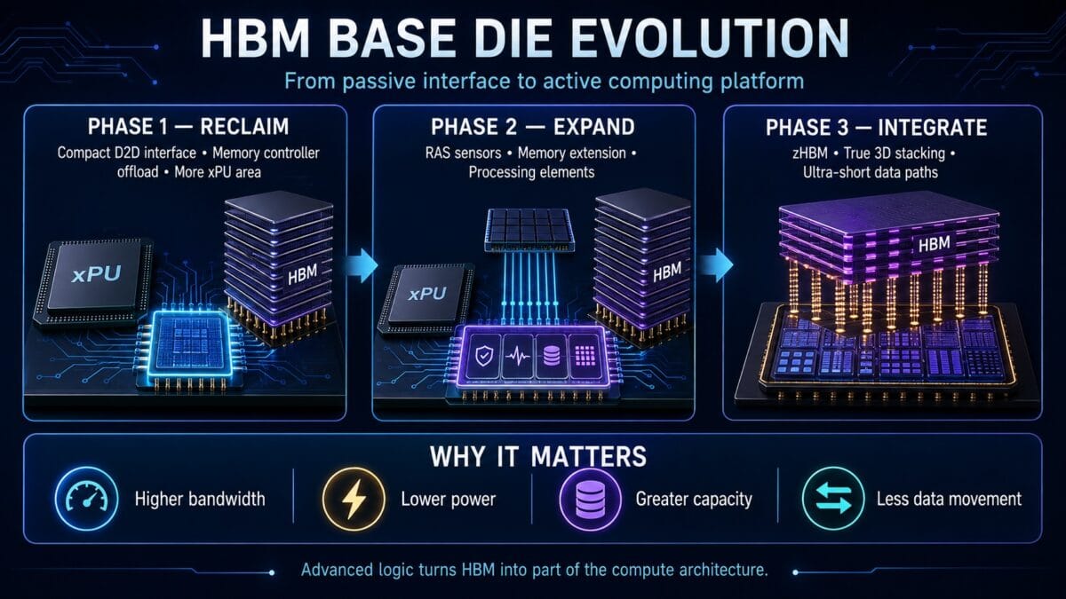
The proposed roadmap has three phases. Phase One reclaims valuable processor area. A compact die-to-die interface replaces the large conventional HBM physical interface, shortening signal paths and improving energy efficiency. The memory controller can then move from the processor into the HBM base die. Samsung also proposes SRAM-based repair logic that can replace defective DRAM rows, potentially improving usable capacity and manufacturing yield. Shrinking the interface, however, raises power density, so heat-path blocks are introduced to conduct heat through the stack and reduce peak temperatures.
제안된 로드맵은 세 단계로 구성되어 있습니다. 1단계는 가치 있는 프로세서 면적을 확보하는 것입니다. 기존의 대형 HBM 물리 인터페이스를 소형 다이 대 다이(die-to-die) 인터페이스로 대체하여 신호 경로를 단축하고 에너지 효율을 향상시킵니다. 이에 따라 메모리 컨트롤러를 프로세서에서 HBM 베이스 다이 내부로 이동시킬 수 있습니다. 또한 삼성은 결함이 있는 DRAM 행을 대체할 수 있는 SRAM 기반 수리 로직을 제안하여, 사용 가능한 용량과 제조 수율을 향상시킬 수 있도록 했습니다. 다만 인터페이스를 축소하면 전력 밀도가 높아지므로, 스택을 통해 열을 배출하고 최고 온도를 낮추기 위한 히트 패스 블록(heat-path blocks)이 도입됩니다.
Phase Two exploits silicon that would otherwise be used mostly for routing. The base die could incorporate thermal, voltage, process, and aging sensors for real-time reliability, availability, and serviceability monitoring. On-die testing and pattern generation could improve fault coverage and yield. Dedicated controllers and interfaces could connect HBM directly to external memory, providing greater capacity with better bandwidth and latency than PCIe-based expansion. Processing elements could also move into the base die, reducing data movement across the interposer. Samsung calls this compute-enhanced form “advanced HBM,” or aHBM.
2단계는 주로 라우팅에 사용되던 실리콘 영역을 활용합니다. 베이스 다이에 온도, 전압, 공정, 열화 센서를 통합하여 실시간 신뢰성, 가용성, 유지보수성(RAS) 모니터링을 구현할 수 있습니다. 다이 내부 테스트 및 패턴 생성을 통해 결함 커버리지와 수율을 높일 수 있습니다. 전용 컨트롤러와 인터페이스를 통해 HBM을 외부 메모리에 직접 연결함으로써, PCIe 기반 확장보다 더 나은 대역폭과 지연 시간으로 더 큰 용량을 제공할 수 있습니다. 연산 요소를 베이스 다이 내부로 이동시켜 인터포저를 가로지르는 데이터 이동을 줄일 수도 있습니다. 삼성은 이러한 연산 강화 형태를 ‘첨단 HBM(aHBM)’이라고 부릅니다.
Phase Three proposes zHBM, a true 3D architecture in which processor logic sits vertically beneath the DRAM stack. Distributed connections would shorten internal data paths and eliminate conventional high-power serial interfaces. Samsung estimates that eliminating this overhead could reduce HBM I/O power by about 70 percent. Achieving zHBM would require wafer-on-wafer assembly, hybrid copper bonding, and a unified design and verification process spanning processor logic, DRAM, packaging, timing, power, signal integrity, and testing.
3단계는 프로세서 로직이 DRAM 스택 수직 아래에 위치하는 진정한 3D 아키텍처인 zHBM을 제안합니다. 분산 연결은 내부 데이터 경로를 단축하고 기존의 고전력 직렬 인터페이스를 없애줍니다. 삼성이 추상한 바에 따르면 이러한 오버헤드를 제거할 경우 HBM I/O 전력을 약 70퍼센트까지 줄일 수 있습니다. zHBM을 달성하기 위해서는 웨이퍼 온 웨이퍼(wafer-on-wafer) 조립, 하이브리드 구리 본딩, 그리고 프로세서 로직, DRAM, 패키징, 타이밍, 전력, 신호 무결성, 테스트를 아우르는 통합 설계 및 검증 프로세스가 필요합니다.
Why does this matter? Modern AI performance increasingly depends not only on computing capacity but on moving and storing data efficiently. Longer context windows, larger key-value caches, and memory-intensive inference make bandwidth, capacity, and energy central system constraints. If Samsung’s roadmap succeeds, HBM will cease to be a relatively passive component selected after processor design. It will become part of the computing architecture itself.
이것이 중요한 이유는 무엇일까요? 현대의 AI 성능은 연산 능력뿐만 아니라 데이터를 얼마나 효율적으로 이동시키고 저장하느냐에 점점 더 크게 의존하고 있습니다. 더 긴 컨텍스트 윈도우, 더 커진 키-값 캐시, 그리고 메모리 집약적인 추론 작업으로 인해 대역폭, 용량, 에너지는 핵심적인 시스템 제약 사항이 되고 있습니다. 삼성이 제안한 로드맵이 성공한다면, HBM은 프로세서 설계 이후에 선택되는 상대적으로 수동적인 부품에서 벗어나 컴퓨팅 아키텍처 그 자체의 일부로 자리 잡게 될 것입니다.
Bottom line: That shift could yield faster AI systems without relying solely on larger processors or more power. It could improve yield, free expensive processor area, reduce data movement, expand capacity, and support workload-specific acceleration. Just as importantly, it would change industry relationships: memory vendors, processor designers, foundries, and packaging specialists would need to co-design products much earlier. The base die therefore represents both a technical opportunity and a strategic battleground. Whoever controls its logic, interfaces, and integration may influence how the next generation of AI systems is built—and how efficiently it scales.
결론적으로, 이러한 변화는 더 큰 프로세서나 더 많은 전력에만 의존하지 않고도 더 빠른 AI 시스템을 구현할 수 있게 해줍니다. 이는 수율을 향상시키고, 비싼 프로세서 면적을 확보하며, 데이터 이동을 줄이고, 용량을 확장하며, 워크로드 맞춤형 가속을 지원할 수 있습니다. 이와 함께 메모리 공급업체, 프로세서 설계자, 파운드리, 패키징 전문가들이 제품을 훨씬 더 이 단계에서부터 공동 설계해야 하므로 산업 생태계의 관계 구조에도 변화가 생기게 됩니다. 따라서 베이스 다이는 기술적 기회이자 전략적 격전지이며, 그 로직, 인터페이스, 통합을 장악하는 주체가 차세대 AI 시스템의 구축 방식과 효율적 확장을 주도하게 될 것입니다.
Source: Sangwook Han, Samsung Memory Business, “HBM Base Die: How HBM Will Evolve Using Advanced Logic Processes,” August 23, 2026.



