Inside the Package Powering Modern AI
Source: https://semiwiki.com/semiconductor-manufacturers/tsmc/371610-inside-the-package-powering-modern-ai/
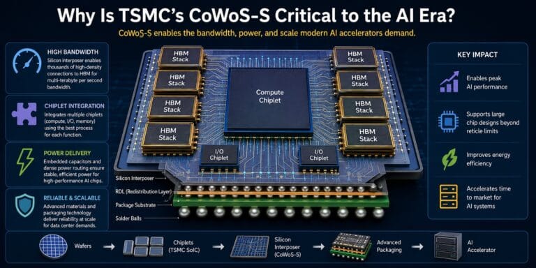
TSMC’s CoWoS-S is critical to the artificial intelligence era because it solves the central systems problem facing modern accelerators: computing capability is growing faster than conventional packages can supply data, power, and connectivity. CoWoS-S, meaning Chip-on-Wafer-on-Substrate with a silicon interposer, is a 2.5D integration platform that places large logic dies or chiplets beside multiple high-bandwidth-memory stacks, then connects them through dense wiring fabricated in silicon.
TSMC의 CoWoS-S는 현대 가속기가 직면한 핵심 시스템 문제, 즉 컴퓨팅 성능이 기존 패키지가 데이터를 공급하고 전력 및 연결성을 제공하는 속도보다 더 빠르게 성장하고 있다는 문제를 해결하기 때문에 인공지능(AI) 시대에 매우 중요합니다. 실리콘 인터포저를 활용하는 칩온웨이퍼온서브스트레이트(Chip-on-Wafer-on-Substrate)를 뜻하는 CoWoS-S는 대형 로직 다이 또는 칩렛을 여러 개의 고대역폭 메모리(HBM) 스택 옆에 배치한 다음, 실리콘으로 제작된 고밀도 배선으로 이들을 연결하는 2.5차원(2.5D) 통합 플랫폼입니다.
AI training and inference depend on moving enormous parameter, activation, and key-value-cache datasets between processors and memory. A leading-edge GPU may contain vast arithmetic throughput, but those units deliver useful performance only when memory bandwidth remains high and communication latency stays low. Ordinary organic substrates cannot provide enough fine-pitch interconnects between a processor and several HBM stacks. CoWoS-S uses a silicon interposer whose routing density is much closer to on-chip metallization. Thousands of short, wide parallel connections can therefore link logic and HBM, producing multi-terabyte-per-second memory interfaces with lower energy per transferred bit than board-level memory.
AI 학습과 추론은 프로세서와 메모리 간에 방대한 양의 매개변수, 활성화 값, 키-밸류(Key-Value) 캐시 데이터셋을 이동시키는 작업에 크게 좌우됩니다. 최첨단 GPU는 엄청난 연산 처리량을 담아낼 수 있지만, 그러한 유닛들은 메모리 대역폭이 높게 유지되고 통신 지연이 낮을 때만 유용한 성능을 발휘합니다. 일반적인 유기 기판은 프로세서와 여러 HBM 스택 사이에 충분한 미세 피치 상호 연결을 제공할 수 없습니다. CoWoS-S는 라우팅 밀도가 온칩 금속화 공정에 훨씬 가까운 실리콘 인터포저를 사용합니다. 따라서 수천 개의 짧고 넓은 병렬 연결을 통해 로직과 HBM을 연결할 수 있으며, 보드 레벨 메모리보다 전송된 비트당 에너지 소비는 낮으면서 초당 수 테라바이트에 달하는 메모리 인터페이스를 구현할 수 있습니다.
The interposer also enables integration beyond the lithographic reticle limit. Manufacturing one enormous monolithic die is constrained by exposure area, defect density, yield, and cost. CoWoS-S allows designers to divide a system into compute, input/output, cache, networking, or specialized chiplets and integrate known-good dies within one package. Each component can use the process node best suited to its function. Compute tiles may use an advanced node, while interface or analog functions use mature nodes. This heterogeneous approach improves yield, design reuse, product segmentation, and time to market without sacrificing package-level bandwidth.
또한 이 인터포저는 노광기 레티클(reticle) 한계를 넘어선 통합을 가능하게 합니다. 하나의 거대한 단일(monolithic) 다이를 제조하는 것은 노광 면적, 결함 밀도, 수율, 비용의 제약을 받습니다. CoWoS-S를 사용하면 설계자가 시스템을 연산, 입출력(I/O), 캐시, 네트워킹 또는 특수 칩렛으로 분할하고, 하나의 패키지 내에서 양품으로 판정된 다이(known-good dies)를 통합할 수 있습니다. 각 구성 요소는 그 기능에 가장 적합한 공정 노드를 사용할 수 있습니다. 연산 타일은 첨단 노드를 사용하는 반면, 인터페이스나 아날로그 기능은 성숙 노드를 사용할 수 있습니다. 이러한 이종(heterogeneous) 접근 방식은 패키지 수준의 대역폭을 희생하지 않으면서도 수율, 설계 재사용, 제품 세분화, 그리고 출시 소요 시간(time to market)을 개선합니다.
Power delivery is equally important. AI accelerators draw extreme current and experience rapid load transients. Voltage droop can reduce clock frequency, corrupt operation, or force conservative power margins. CoWoS-S incorporates dense power-routing structures and embedded deep-trench capacitors in the silicon interposer. These capacitors provide local charge near the logic dies, improving power integrity at frequencies where motherboard capacitors and package components respond too slowly. Short interconnects also reduce parasitic resistance and inductance, supporting stable operation at high power.
전력 공급 역시 그못지않게 중요합니다. AI 가속기는 극도로 높은 전류를 소모하며 급격한 부하 과도 현상을 겪습니다. 전압 강하(Voltage droop)는 클록 주파수를 떨어뜨리거나, 작동 오류를 일으키거나, 보수적인 전력 마진을 강제할 수 있습니다. CoWoS-S는 실리콘 인터포저 내부에 고밀도 전력 라우팅 구조와 매립형 심천 트렌치 커패시터(deep-trench capacitors)를 통합하고 있습니다. 이 커패시터들은 로직 다이 근처에 국부적인 전하를 공급하여, 마더보드 커패시터와 패키지 구성 요소가 너무 느리게 반응하는 주파수 대역에서 전력 무결성(power integrity)을 향상시킵니다. 또한 짧은 상호 연결은 기생 저항과 인덕턴스를 줄여주어 높은 전력 환경에서도 안정적인 작동을 지원합니다.
Thermal and mechanical engineering make the platform difficult to reproduce. A large interposer carrying several dies must survive wafer processing, micro-bump bonding, molding, substrate attachment, thermal cycling, and sustained data-center operation. Differences in thermal expansion among silicon, copper, underfill, molding compounds, and organic substrates create warpage and stress. TSMC’s value lies not merely in the interposer concept, but in controlling materials, assembly accuracy, yield, test, reliability, and high-volume manufacturing across the entire process.
열 및 기계 공학적 요소는 이 플랫폼을 쉽게 모방하기 어렵게 만드는 원인입니다. 여러 개의 다이를 탑재한 대형 인터포저는 웨이퍼 공정, 마이크로 범프 본딩, 몰딩, 기판 부착, 열 순환, 그리고 장기간 지속되는 데이터 센터 가동을 모두 견뎌내야 합니다. 실리콘, 구리, 언더필, 몰딩 컴파운드, 유기 기판 간의 열팽창 차이는 휨(warpage)과 응력을 유발합니다. TSMC의 진정한 가치는 단순히 인터포저라는 개념 자체에 있는 것이 아니라, 전체 공정에 걸쳐 소재, 조립 정밀도, 수율, 테스트, 신뢰성, 그리고 대량 생산을 통제하는 역량에 있습니다.
Scale further strengthens CoWoS-S. TSMC reports that the platform has been in production since 2012 and supports silicon interposers reaching approximately 3.3 times reticle size. Its fifth-generation implementation demonstrated an interposer of about 2,500 square millimeters, capable of accommodating multiple logic chips and eight HBM stacks. Such dimensions transform the package into a system-level integration platform rather than a protective enclosure.
규모의 경제는 CoWoS-S를 더욱 강화합니다. TSMC에 따르면 이 플랫폼은 2012년부터 생산되어 왔으며, 레티클 크기의 약 3.3배에 달하는 실리콘 인터포저를 지원합니다. 5세대 구현에서는 약 2,500제곱밀리미터 크기의 인터포저를 선보였으며, 이는 다수의 로직 칩과 8개의 HBM 스택을 수용할 수 있는 능력을 갖추고 있습니다. 이러한 치수는 패키지를 단순한 보호용 외장이 아니라 시스템 수준의 통합 플랫폼으로 탈바꿈시킵니다.
Its maturity also lowers commercialization risk. Customers receive an ecosystem spanning design rules, interposer fabrication, die assembly, thermal solutions, electrical verification, and production testing. That integration shortens debugging cycles and makes multi-die accelerators manufacturable at hyperscale. Few suppliers can match the combination of leading-edge foundry access, packaging precision, capacity investment, and customer trust.
또한 이러한 성숙도는 상용화 위험을 낮춰줍니다. 고객은 설계 규칙, 인터포저 제조, 다이 조립, 열 관리 솔루션, 전기적 검증, 그리고 양산 테스트를 아우르는 생태계를 제공받습니다. 이러한 통합은 디버깅 주기를 단축시키고 하이퍼스케일 규모에서 멀티 다이 가속기의 양산을 가능하게 만듭니다. 최첨단 파운드리 접근성, 패키지 정밀도, 설비 투자, 그리고 고객의 신뢰를 이만큼 조합할 수 있는 공급업체는 거의 없습니다.
CoWoS-S is therefore a strategic bottleneck. Advanced logic wafers and HBM may be available, yet an AI accelerator cannot ship until those components are assembled, bonded, tested, and qualified as one reliable package. Packaging capacity consequently determines how quickly cloud providers can deploy new computing clusters. It also shapes accelerator architecture because interposer area, HBM placement, bump pitch, power density, substrate size, and cooling limits must be co-designed years before production.
따라서 CoWoS-S는 전략적 병목 구간입니다. 첨단 로직 웨이퍼와 HBM을 확보했더라도, AI 가속기는 이 구성 요소들이 하나의 신뢰할 수 있는 패키지로 조립, 본딩, 테스트, 적격성 평가를 거치기 전에는 출하될 수 없습니다. 결과적으로 패키징 생산 능력은 클라우드 서비스 제공업체들이 새로운 컴퓨팅 클러스터를 얼마나 빠르게 구축할 수 있는지를 결정합니다. 또한 인터포저 면적, HBM 배치, 범프 피치, 전력 밀도, 기판 크기, 냉각 한계 등이 생산 수년 전에 함께 설계(co-designed)되어야 하므로 가속기 아키텍처의 형태까지 좌우합니다.
Bottom line: The importance of CoWoS-S ultimately reflects a broader semiconductor transition. Transistor scaling remains valuable, but system performance increasingly depends on how efficiently multiple dies, memories, power networks, and communication links are integrated. In the AI era, the package has become part of the computing architecture. CoWoS-S is critical because it converts separately manufactured silicon into a tightly coupled, bandwidth-rich, energy-efficient computing system.
요약하자면: CoWoS-S의 중요성은 궁극적으로 더 넓은 반도체 전환기를 반영합니다. 트렌치 스케일링은 여전히 가치가 있지만, 시스템 성능은 다수의 다이, 메모리, 전력 네트워크, 통신 링크가 얼마나 효율적으로 통합되는가에 점점 더 의존하고 있습니다. AI 시대에 패키지는 이제 컴퓨팅 아키텍처의 일부가 되었습니다. CoWoS-S가 결정적으로 중요한 이유는 따로 제조된 실리콘을 긴밀하게 결합되고 대역폭이 풍부하며 에너지 효율적인 컴퓨팅 시스템으로 변환해 주기 때문입니다.



