Intel Foundry: AI performance now depends on the whole system
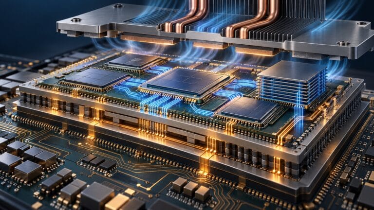
For decades, chipmakers improved computing performance largely by putting more capable circuitry on a piece of silicon. That remains important, but AI is exposing its limits. Large models demand enormous amounts of data movement, sustained power and effective cooling. A fast processor cannot deliver its full benefit if memory cannot feed it quickly enough or heat forces it to slow down.
수십 년 동안 칩 제조업체들은 주로 실리콘 웨이퍼 위에 더 뛰어난 회로를 집적하는 방식으로 컴퓨팅 성능을 향상시켜 왔습니다. 그 방식은 여전히 중요하지만, AI는 그 한계를 드러내고 있습니다. 거대 모델들은 엄청난 양의 데이터 이동, 지속적인 전력 공급, 그리고 효과적인 냉각을 요구합니다. 메모리가 프로세서에 데이터를 충분히 빨리 공급하지 못하거나 발열로 인해 성능을 낮춰야 한다면, 아무리 빠른 프로세서라도 그 진정한 이점을 발휘할 수 없습니다.
In a September 2026 article, Intel Foundry’s Lalitha Immaneni argues that the next gains will come from designing silicon, packaging, circuit boards and the wider platform as one system, to which I agree with 100%. Advanced packaging is central to that approach. Once chiefly a way to protect a finished chip and connect it to a board, the package now helps determine how processors communicate with memory, how power reaches them and how heat escapes.
2026년 9월 기사에서 인텔 파운드리의 랄리타 이마네니(Lalitha Immaneni)는 다음 단계의 성능 향상은 실리콘, 패키징, 회로 기판, 그리고 더 넓은 플랫폼을 하나의 시스템으로 설계하는 데서 올 것이라고 주장했으며, 저자 역시 이에 전적으로 동의합니다. 첨단 패키징은 이러한 접근 방식의 핵심입니다. 과거에는 주로 완성된 칩을 보호하고 기판에 연결하는 수단이었던 패키지가, 이제는 프로세서가 메모리와 통신하는 방식, 전력이 공급되는 방식, 그리고 열이 빠져나가는 방식을 결정하는 데 도움을 줍니다.
One way to build such systems is to divide a large design into smaller chiplets. Different chiplets can perform different jobs and can be made with the manufacturing processes best suited to each. Designers may be able to reuse existing components, combine technologies and build products that would be impractical as a single piece of silicon. But dividing a chip creates new questions: where should each function go, how should the pieces connect and what will those connections cost in power, space and speed?
이러한 시스템을 구축하는 한 가지 방법은 대형 설계를 더 작은 칩렛(chiplets)으로 쪼개는 것입니다. 서로 다른 칩렛들은 각각 다른 역할을 수행할 수 있으며, 각 역할에 가장 적합한 제조 공정으로 제작될 수 있습니다. 설계자들은 기존 부품을 재사용하고, 기술을 결합하며, 단일 실리콘 조각으로는 구현하기 비현실적인 제품을 만들 수 있게 됩니다. 그러나 칩을 쪼개면 새로운 질문들이 생겨납니다. 각 기능이 어디로 가야 하는지, 조각들은 어떻게 연결되어야 하는지, 그리고 그 연결은 전력, 공간, 속도 측면에서 어떤 비용을 치르게 되는지 등이 그것입니다.
Those questions matter especially for AI hardware. A processor might be capable of more calculations than its memory connection can support. Moving components closer together may improve communication while concentrating heat. A package that works electrically may prove difficult to manufacture reliably. Improving one part of the design can worsen another, so the best choice often becomes clear only when the complete system is evaluated.
이러한 질문들은 특히 AI 하드웨어에서 매우 중요합니다. 프로세서가 메모리 연결이 감당할 수 있는 것보다 더 많은 연산을 처리할 수 있는 역량을 가졌을 수도 있습니다. 컴포넌트들을 서로 더 가깝게 배치하면 통신은 개선되겠지만 열이 집중될 수 있습니다. 전기적으로 잘 작동하는 패키지도 안정적으로 제조하기는 어려울 수 있습니다. 설계의 한 부분을 개선하면 다른 부분이 악화될 수 있기 때문에, 가장 최선의 선택은 대개 전체 시스템이 평가될 때 비로소 명확해집니다.
Immaneni calls for that evaluation to begin early. Before committing to a design, teams should compare ways to divide functions among chiplets, choose manufacturing processes, route connections and integrate memory. They also need to test likely effects on temperature, power delivery, manufacturing yield and cost. Discovering a problem while exploring designs is far less disruptive than finding it after detailed layouts or physical prototypes are complete.
이마네니는 이러한 평가가 조기에 시작되어야 한다고 촉구합니다. 팀들은 설계에 착수하기 전에 칩렛 간 기능을 나누는 방법, 제조 공정 선택, 연결 라우팅, 메모리 통합 방식을 비교해야 합니다. 또한 온도, 전력 공급, 수율, 비용에 미칠 잠재적 영향도 테스트해야 합니다. 설계 탐색 단계에서 문제를 발견하는 것은 상세 레이아웃이나 물리적 시제품이 완성된 후에 문제를 발견하는 것보다 훨씬 파급 효과가 적습니다.
Connections between chiplets are a case in point. They require more than a shared communication specification. The positions and spacing of physical contacts must fit the package, and engineers must establish that signals work under real operating conditions. If chiplets from different suppliers are to combine easily, compatible interfaces, reliable design information and validated components will be essential. Otherwise, each new combination risks becoming a costly custom project.
칩렛 간의 연결이 좋은 예입니다. 이는 단순히 공통된 통신 사양 그 이상을 요구합니다. 물리적 접점의 위치와 간격이 패키지에 맞아야 하며, 엔지니어들은 실제 작동 조건에서 신호가 제대로 작동하는지 확인해야 합니다. 서로 다른 공급업체의 칩렛들이 쉽게 결합하려면 호환 가능한 인터페이스, 신뢰할 수 있는 설계 정보, 그리고 검증된 부품이 필수적입니다. 그렇지 않으면 새로운 조합마다 비용이 많이 드는 맞춤형 프로젝트가 될 위험이 있습니다.
Heat and power add further constraints. AI systems can operate near peak activity for long periods, creating concentrated hot spots. The location of chiplets and the materials around them affect cooling. Likewise, the path that delivers electricity through the board, package and silicon affects how much performance a system can sustain. These are architectural choices, not finishing touches.
열과 전력은 추가적인 제약 요인입니다. AI 시스템은 오랜 시간 동안 최고 작동 상태 근처에서 구동될 수 있으며, 이는 집중된 핫스팟(hot spots)을 만들어냅니다. 칩렛의 위치와 그 주변 소재들은 냉각에 영향을 미칩니다. 마찬가지로 기판, 패키지, 실리콘을 통과해 전기를 전달하는 경로는 시스템이 유지할 수 있는 성능 수준에 영향을 줍니다. 이것들은 마무리 단계의 사소한 작업이 아니라 아키텍처적 선택입니다.
That changes how engineers must work together. In a largely sequential process, chip designers could make decisions and pass a design to package and board teams later. Tightly integrated systems require those groups to compare options and resolve conflicts throughout development. Better simulation, experimentally checked models and digital representations of proposed systems could help teams predict problems before building expensive hardware.
이러한 변화는 엔지니어들이 협업하는 방식도 바꾸어 놓습니다. 대체로 순차적인 프로세스에서는 칩 설계자들이 결정을 내린 뒤 나중에 패키지 및 보드 팀에 설계를 넘겨주곤 했습니다. 하지만 긴밀하게 통합된 시스템에서는 이 그룹들이 개발 과정 전반에 걸쳐 옵션을 비교하고 충돌을 해결해야 합니다. 더 나은 시뮬레이션, 실험적으로 검증된 모델, 그리고 제안된 시스템의 디지털 표현은 엔지니어링 팀이 비싼 하드웨어를 구축하기 전에 문제를 예측하는 데 도움을 줄 수 있습니다.
Intel Foundry points to its packaging technologies and supporting design tools as part of this effort. The broader challenge, however, reaches beyond any one supplier. Foundries, packaging specialists, software toolmakers, memory suppliers and customers need ways to exchange trustworthy design information and make components work together.
인텔 파운드리는 이러한 노력의 일환으로 자사의 패키징 기술과 지원 설계 도구들을 강조합니다. 그러나 더 큰 과제는 특정 공급업체 하나를 넘어섭니다. 파운드리, 패키징 전문가, 소프트웨어 툴메이커, 메모리 공급업체, 그리고 고객들은 신뢰할 수 있는 설계 정보를 교환하고 부품들이 서로 유기적으로 작동하게 만들 수 있는 방법이 필요합니다.
Bottom line: Demand for AI computing is rising, but more processing circuitry alone cannot solve limits in bandwidth, energy use and heat. Designing the whole system together could yield faster, more efficient products and reduce late redesigns. Intel Foundry’s focus on system-level co-design and ecosystem collaboration reflects this industry shift. The approach will succeed only if engineers can model those interactions accurately and make chiplets practical to combine at scale.
요약하자면: AI 컴퓨팅에 대한 수요는 증가하고 있지만, 단순히 처리 회로를 늘리는 것만으로는 대역폭, 에너지 소비, 발열의 한계를 해결할 수 없습니다. 전체 시스템을 함께 설계하면 더 빠르고 효율적인 제품을 만들 수 있으며 늦은 재설계를 줄일 수 있습니다. 시스템 레벨의 공동 설계와 생태계 협업에 초점을 맞추는 인텔 파운드리의 행보는 이러한 산업적 변화를 반영합니다. 이 접근 방식은 엔지니어들이 이러한 상호작용을 정확하게 모델링하고 칩렛들을 대규모로 실용적으로 결합할 수 있을 때만 성공할 수 있습니다.



