Intel’s Tiny Bridges Could Lead to Very Big Paychecks
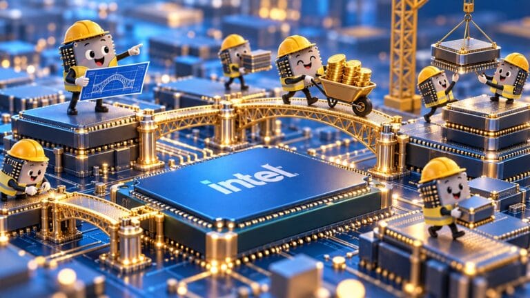
Intel’s next big opportunity could come from something that sounds spectacularly unglamorous: connecting tiny pieces of silicon. Advanced packaging rarely attracts the attention lavished on powerful processors or artificial intelligence models. Yet it increasingly determines how effectively those technologies perform. For Intel, making separate chips behave like one tightly integrated system could become a valuable business of its own.
인텔(Intel)의 다음 대형 기회는 보기에는 전혀 화려하지 않은 것, 즉 아주 작은 실리콘 조각들을 서로 연결하는 것에서 올 수 있습니다. 어드밴스드 패키징(고성능 패키징)은 강력한 프로세서나 인공지능 모델에 쏟아지는 관심은 거의 받지 못하지만, 그러한 기술들이 얼마나 효과적으로 성능을 발휘하는지를 점점 더 크게 좌우하고 있습니다. 인텔에게 있어 서로 다른 칩들이 마치 하나의 긴밀하게 통합된 시스템처럼 작동하도록 만드는 것은 그 자체로 가치 있는 사업이 될 수 있습니다.
The logic starts with a practical problem. AI systems need enormous computing power, fast memory and efficient communication between components. Building everything into one gigantic chip becomes increasingly difficult and expensive. Instead, designers can divide a processor into smaller chiplets, manufacture different pieces using suitable technologies, then connect them inside a single package. The connections become central to the finished product’s capabilities.
이러한 논리의 시작은 현실적인 문제에 있습니다. AI 시스템은 엄청난 연산 능력, 빠른 메모리, 그리고 컴포넌트 간의 효율적인 통신을 필요로 합니다. 이 모든 것을 하나의 거대한 칩으로 만드는 것은 점점 더 어려워지고 비용도 많이 듭니다. 대신 설계자들은 프로세서를 더 작은 칩렛으로 나누어 적합한 기술로 각각 제조한 후, 하나의 패키지 안에서 이들을 연결할 수 있습니다. 이때 이 연결 부위가 최종 제품 성능의 핵심이 됩니다.
This is where Intel’s alphabet soup gets interesting. EMIB, short for Embedded Multi-die Interconnect Bridge, uses small silicon bridges embedded in a package substrate to connect neighboring chips. Rather than placing a large silicon connection layer beneath the entire assembly, Intel concentrates dense connections where they are needed. The company argues that this approach offers advantages in cost, flexibility and scaling.
여기서 인텔의 다양한 약어 기술들이 흥미로워집니다. 임베디드 멀티다이 인터커넥트 브리지(EMIB, Embedded Multi-die Interconnect Bridge)는 패키지 기판에 내장된 작은 실리콘 브리지를 사용해 인접한 칩들을 연결합니다. 전체 어셈블리 하단에 커다란 실리콘 연결 레이어를 배치하는 대신, 인텔은 필요한 곳에 조밀한 연결을 집중시킵니다. 인텔은 이 접근 방식이 비용, 유연성, 확장성 측면에서 이점을 제공한다고 주장합니다.
Foveros adds another dimension by allowing chiplets to be stacked vertically. Think of EMIB as connecting buildings across a neighborhood and Foveros as adding floors. Together, these technologies give designers more ways to combine computing, memory and other functions. Intel’s newer EMIB-T technology also introduces connections through its bridges, improving power delivery and supporting the bandwidth requirements of increasingly ambitious systems.
포베로스(Foveros)는 칩렛을 수직으로 적층할 수 있게 함으로써 또 다른 차원을 더해줍니다. EMIB가 동네 사이의 건물들을 연결하는 것이라면, 포베로스는 건물의 층을 높이는 것으로 비유할 수 있습니다. 이 기술들을 통해 설계자들은 연산, 메모리 및 기타 기능들을 결합할 수 있는 더 많은 방법을 확보하게 됩니다. 인텔의 최신 EMIB-T 기술은 브리지를 관통하는 연결 방식도 도입하여 전력 공급을 개선하고 점점 더 야심찬 시스템의 대역폭 요구 사항을 지원합니다.
The commercial attraction extends beyond Intel’s own processors. Its packaging services can integrate chiplets produced using different manufacturing technologies and foundries. A customer could therefore use Intel to assemble a sophisticated product without committing every component to Intel’s wafer factories. That creates a potentially useful entry point: customers can purchase a specific capability while keeping flexibility elsewhere in their supply chains.
상업적 매력은 인텔 자체 프로세서에만 국한되지 않습니다. 인텔의 패키징 서비스는 서로 다른 제조 기술과 파운드리를 통해 생산된 칩렛들을 통합할 수 있습니다. 따라서 고객은 모든 컴포넌트를 인텔의 웨이퍼 공장에 전적으로 맡기지 않고도 인텔을 통해 정교한 제품을 조립할 수 있습니다. 이는 잠재적으로 유용한 진입점을 제공합니다. 고객들은 공급망의 다른 부분에서는 유연성을 유지하면서 특정 역량만을 구매할 수 있기 때문입니다.
That distinction matters for Intel’s wider manufacturing ambitions. Winning an entire processor manufacturing contract requires customers to make consequential technical and commercial commitments. Packaging offers another way to begin working together. Intel itself has described customers approaching first for advanced packaging, with successful execution helping build confidence in its broader foundry services. The opportunity is both immediate business and a foundation for deeper relationships.
이러한 차별점은 인텔의 더 넓은 제조 분야 야망에 매우 중요합니다. 프로세서 제조 계약 전체를 수주하려면 고객이 중대한 기술적 및 상업적 약속을 감수해야 합니다. 반면 패키징은 협력을 시작할 수 있는 또 다른 방법을 제시합니다. 인텔은 고객들이 어드밴스드 패키징을 위해 먼저 접근해 오며, 성공적인 실행이 더 광범위한 파운드리 서비스에 대한 신뢰를 구축하는 데 도움을 준다고 설명한 바 있습니다. 이 기회는 당장의 사업인 동시에 더 깊은 관계로 나아가는 토대이기도 합니다.
The billions in the headline represent potential, rather than established packaging revenue. Growing demand for complex AI systems creates an opening for suppliers that can integrate more components reliably and economically. Intel’s technical roadmap targets substantially larger assemblies, including configurations accommodating at least sixteen high-bandwidth memory stacks by 2028. Those plans illustrate the scale of the systems it hopes to serve; they remain forward-looking development targets.
기사 제목에 등장하는 수십억 달러는 확정된 패키징 매출이라기보다는 잠재력을 나타냅니다. 복잡한 AI 시스템에 대한 수요 증가로 인해 더 많은 컴포넌트를 안정적이고 경제적으로 통합할 수 있는 공급업체들에게 새로운 길이 열리고 있습니다. 인텔의 기술 로드맵은 2028년까지 최소 16개의 고대역폭 메모리(HBM) 스택을 수용하는 구성을 포함하여, 실질적으로 더 커진 어셈블리를 목표로 하고 있습니다. 이러한 계획들은 인텔이 서비스하고자 하는 시스템의 규모를 보여주며, 여전히 미래 지향적인 개발 목표로 남아 있습니다.
Intel has also given the effort organizational weight. In June 2026, it appointed semiconductor veteran Seok-Hee Lee to lead advanced packaging, system integration and related manufacturing activities. Establishing dedicated leadership signals that packaging is becoming a focused business priority, with execution and customer delivery receiving attention alongside the underlying engineering. The appointment supports the strategy, although leadership changes alone cannot guarantee commercial success.
또한 인텔은 이러한 노력에 조직적인 힘을 실어주었습니다. 2026년 6업체, 인텔은 어드밴스드 패키징, 시스템 통합 및 관련 제조 활동을 이끌 팹더 반도체 베테랑 이석희를 임명했습니다. 전담 리더십을 구축한 것은 패키징이 핵심적인 사업 우선순위가 되고 있으며, 기초적인 엔지니어링과 함께 실행 및 고객 인도 역시 주목받고 있음을 시사합니다. 이 인사는 전략을 뒷받침하지만, 리더십 변화만으로는 상업적 성공을 보장할 수 없습니다.
There are substantial hurdles. Complex packages must meet demanding standards for manufacturing yield, heat management, testing and reliability. Customers need confidence that Intel can deliver consistently at production scale. Revenue will depend on actual design wins, volumes and pricing, while profits will also reflect investment and operating costs. Technical promise, however impressive, must translate into products that customers can ship economically.
상당한 난관들도 존재합니다. 복잡한 패키지는 제조 수율, 열 관리, 테스트 및 신뢰성에 대한 까다로운 표준을 충족해야 합니다. 고객들은 인텔이 생산 규모에서 일관되게 제품을 공급할 수 있다는 확신이 필요합니다. 매출은 실제 디자인 윈(수주), 물량, 가격에 따라 좌우될 것이며, 수익 역시 투자 비용과 운영 비용을 반영할 것입니다. 기술적 잠재력이 아무리 인상적이라 해도, 고객이 경제적으로 출하할 수 있는 제품으로 구현되어야 합니다.
Bottom line: Intel does not need to design every winning AI chip to benefit from AI infrastructure spending. It can supply the intricate connections that help other companies’ designs work. If those capabilities earn sustained customer trust, this deeply nerdy manufacturing specialty could become a meaningful growth engine, turning microscopic bridges into a much larger commercial opportunity.
결론적으로, 인텔이 AI 인프라 지출로부터 혜택을 받기 위해 모든 성공적인 AI 칩을 직접 설계할 필요는 없습니다. 다른 기업들의 설계가 작동할 수 있도록 돕는 복잡한 연결 장치를 공급하면 됩니다. 이러한 역량들이 지속적인 고객의 신뢰를 얻는다면, 이토록 뼛속까지 공학적인 제조 전문 분야는 의미 있는 성장 동력이 되어 미세한 브리지를 훨씬 더 큰 상업적 기회로 탈바꿈시킬 수 있을 것입니다.



