Maskless EUV Lithography: An Alternative to E-Beam
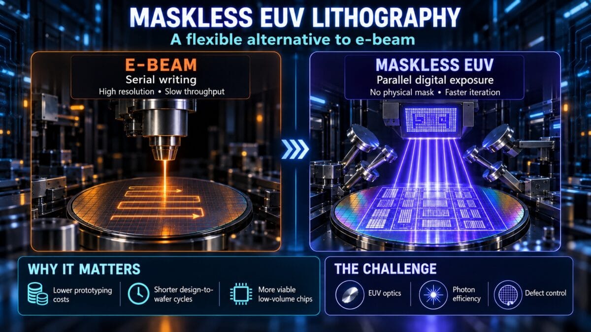
Source: https://semiwiki.com/lithography/373583-maskless-euv-lithography-an-alternative-to-e-beam/
Semiconductor manufacturing depends on lithography: the process of transferring tiny circuit patterns onto a silicon wafer. Conventional extreme-ultraviolet (EUV) lithography projects light with a wavelength of 13.5 nanometers through a reflective optical system, using a custom photomask to define each layer. It can print extraordinarily small features at high throughput, but every new design requires an expensive, carefully manufactured mask set. Maskless EUV lithography proposes a different approach. Instead of storing the pattern on a physical mask, it would use a programmable array or another rapidly addressable optical element to write digital patterns directly onto the wafer.
반도체 제조는 미세한 회로 패턴을 실리콘 웨이퍼에 전사하는 공정인 리소그래피에 의존합니다. 기존의 극자외선(EUV) 리소그래피는 13.5나노미터 파장의 빛을 반사 광학계를 통해 투과시키며, 맞춤형 포토마스크를 사용하여 각 층을 정의합니다. 이 방식은 매우 작은 패턴을 높은 처리량(생산량)으로 인쇄할 수 있지만, 모든 새로운 디자인마다 비용이 많이 들고 정밀하게 제작된 마스크 세트가 필요합니다. 무마스크(Maskless) EUV 리소그래피는 이와 다른 접근 방식을 제안합니다. 패턴을 물리적 마스크에 저장하는 대신, 프로그래밍 가능한 어레이나 빠르게 제어할 수 있는 광학 요소를 사용하여 디지털 패턴을 웨이퍼에 직접 기록하는 방식입니다.
The idea occupies an important middle ground between conventional EUV and electron-beam lithography. E-beam systems are also maskless and can draw extremely fine features, making them essential for research, prototyping, and producing the masks used by optical lithography. Their weakness is speed. An electron beam generally writes patterns serially, point by point or shape by shape. A modern chip contains an immense number of features, so exposing a full wafer can take far too long for practical manufacturing. Parallel multibeam systems improve throughput, but they introduce substantial complexity in beam control, calibration, data handling, and defect management.
이 아이디어는 기존 EUV와 전자빔(e-beam) 리소그래피 사이의 중요한 중간 지점을 차지합니다. 전자빔 시스템 역시 마스크가 필요 없고 극도로 미세한 패턴을 그릴 수 있어 연구, 시제품 제작, 그리고 광학 리소그래피에 사용되는 마스크 제작에 필수적입니다. 단점은 속도입니다. 전자빔은 일반적으로 패턴을 점별로 또는 형상별로 직렬(serial) 방식으로 기록합니다. 현대의 칩에는 엄청나게 많은 패턴 요소가 포함되어 있으므로, 전체 웨이퍼를 노광하는 데 실제 제조용으로는 너무 오랜 시간이 걸릴 수 있습니다. 병렬 멀티빔 시스템은 처리량을 개선하지만, 빔 제어, 보정, 데이터 처리 및 결함 관리 측면에서 상당한 복잡성을 유발합니다.
A maskless EUV platform could combine direct digital patterning with the parallel exposure advantages of light. In principle, millions of controllable elements could expose many features simultaneously, avoiding the serial bottleneck of a single e-beam. Designs could be changed by loading a new pattern file instead of fabricating a new mask. That would shorten iteration cycles and lower the fixed cost of producing small quantities. Researchers could test several layouts quickly, startups could prototype advanced chips without purchasing a complete mask set, and manufacturers could economically produce specialized devices in volumes too low for conventional EUV.
무마스크 EUV 플랫폼은 직접 디지털 패터닝과 빛의 병렬 노광 이점을 결합할 수 있습니다. 원리적으로 수백만 개의 제어 가능한 요소가 동시에 많은 패턴을 노광할 수 있으므로, 단일 전자빔의 직렬 병목 현상을 피할 수 있습니다. 새로운 마스크를 제작하는 대신 새로운 패턴 파일을 로드하는 것만으로 설계를 변경할 수 있습니다. 이를 통해 반복 주기가 단축되고 소량 생산 시의 고정 비용이 절감될 수 있습니다. 연구원들은 여러 레이아웃을 신속하게 테스트할 수 있고, 스타트업은 완전한 마스크 세트를 구매하지 않고도 첨단 칩의 시제품을 제작할 수 있으며, 제조업체는 기존 EUV로는 너무 낮은 물량의 특수 소자를 경제적으로 생산할 수 있습니다.
This flexibility is why the technology matters. Mask costs and lead times increasingly shape who can experiment at the leading edge. When each design revision carries a large upfront expense, companies are encouraged to make fewer, safer bets. Maskless EUV could support more frequent experimentation, customized accelerators, small-batch photonics, secure or locally produced chips, and late-stage personalization. It could also reduce the economic penalty of correcting a design error. In an industry where learning speed is a competitive advantage, faster design-to-wafer cycles may be as valuable as smaller transistors.
이러한 유연성이 바로 이 기술이 중요한 이유입니다. 마스크 비용과 리드 타임(소요 시간)은 점점 더 누가 최첨단 기술을 실험할 수 있는지를 좌우합니다. 모든 디자인 변경에 큰 선행 비용이 소요되면, 기업들은 더 적고 안전한 베팅을 하도록 유도됩니다. 무마스크 EUV는 더 빈번한 실험, 맞춤형 가속기, 소량 배치 포토닉스, 보안 또는 지역 생산 칩, 그리고 후기 개인화(late-stage personalization)를 지원할 수 있습니다. 또한 디자인 오류 수정에 따른 경제적 부담을 줄여줄 수 있습니다. 학습 속도가 경쟁 우위인 산업에서는 더 빠른 디자인-투-웨이퍼(design-to-wafer) 주기가 더 작은 트랜지스터만큼이나 가치 있을 수 있습니다.
The approach, however, is not a simple replacement for either EUV scanners or e-beam tools. EUV radiation is strongly absorbed by most materials, so the system must operate in vacuum and rely on specialized reflective optics. A programmable pattern generator must survive EUV exposure while switching with exceptional precision. It must deliver adequate optical power, maintain nanometer-scale placement accuracy, control heat and contamination, and avoid adding defects. Photoresist behavior creates another challenge: at very small dimensions, limited photon counts produce stochastic variation, including rough edges, missing contacts, or unintended bridges. Vast pattern files must also be processed and delivered in real time.
그러나 이 접근 방식이 EUV 스캐너나 전자빔 장비를 간단히 대체하는 것은 아닙니다. EUV 방사선은 대부분의 물질에 강하게 흡수되므로 시스템은 진공 상태에서 작동해야 하며 특수 반사 광학계에 의존해야 합니다. 프로그래밍 가능한 패턴 생성기는 뛰어난 정밀도로 스위칭하면서 EUV 노광을 견뎌야 합니다. 또한 적절한 광학적 출력을 전달하고, 나노미터 급의 배치 정확도를 유지하며, 열과 오염을 제어하고, 결함 추가를 방지해야 합니다. 포토레지스트(감광액)의 거동은 또 다른 과제를 제기합니다. 매우 작은 치수에서는 제한된 광자 수로 인해 거친 모서리, 누락된 콘택트, 의도치 않은 브리지 등 확률적 변동이 발생합니다. 또한 방대한 패턴 파일을 실러 타임(실시간)으로 처리하고 전달해야 합니다.
For these reasons, the first successful applications would likely be selective rather than a wholesale takeover of high-volume lithography. Maskless EUV may initially serve rapid prototyping, low-volume advanced devices, research, mask repair, or particular critical layers where flexibility justifies lower throughput. E-beam would remain valuable for the finest direct-write work and mask production, while masked EUV would retain its advantage for manufacturing millions of identical chips.
이러한 이유로 최초의 성공적인 응용 분야는 대량 생산 리소그래피를 완전히 대체하기보다는 선별적인 적용이 될 가능성이 높습니다. 무마스크 EUV는 초기에는 빠른 프로토타이핑, 소량 첨단 소자, 연구, 마스크 수리, 또는 유연성이 낮은 처리량을 정당화하는 특정 핵심 층에 기여할 수 있습니다. 전자빔은 가장 미세한 직접 기록 작업과 마스크 제작에 여전히 유용할 것이며, 마스크 기반 EUV는 수백만 개의 동일한 칩을 제조하는 데 있어 우위를 유지할 것입니다.
Bottom line: Even within that narrower role, maskless EUV could change semiconductor innovation. It attacks a growing mismatch: fabrication tools can create remarkable structures, yet the cost and delay of preparing masks restrict access to them. By turning patterns from physical infrastructure into software-controlled inputs, the technology could make advanced lithography more adaptable and accessible. Its importance is therefore not merely technical. Maskless EUV could alter the economics of experimentation, broaden participation in chip design, and help the semiconductor industry move from rigid mass production toward faster, more varied, and more responsive manufacturing for many emerging applications worldwide.
결론적으로, 이러한 제한된 역할 내에서도 무마스크 EUV는 반도체 혁신을 변화시킬 수 있습니다. 이는 점점 심화되는 불일치, 즉 제조 장비는 놀라운 구조를 만들 수 있지만 마스크 준비 비용과 지연이 그 접근을 제한한다는 점을 공략합니다. 패턴을 물리적 인프라에서 소프트웨어 제어 입력으로 전환함으로써 이 기술은 첨단 리소그래피를 더욱 적응력 있고 접근하기 쉽게 만들 수 있습니다. 따라서 그 중요성은 단순히 기술적인 것만이 아닙니다. 무마스크 EUV는 실험의 경제학을 바꾸고, 칩 디자인 참여를 넓히며, 반도체 산업이 엄격한 대량 생산에서 벗어나 전 세계의 다양한 신흥 응용 분야를 위한 더 빠르고 다양하며 유연한 제조로 나아가는 데 도움을 줄 수 있습니다.



