Overcoming the Edge AI Power Wall with Low-Voltage Foundation IP
As artificial intelligence (AI) workloads migrate to endpoint hardware, edge AI devices face immense pressure to deliver real-time inference within highly restrictive power and thermal envelopes. Traditional silicon scaling no longer yields the power-density returns it once did. To compensate, engineering teams are turning to aggressive voltage scaling. Lowering supply voltages down to near-threshold operating points unlocks step-function gains in performance-per-watt.
인공지능(AI) 워크로드(작업 부하)가 엔드포인트 하드웨어로 이동함에 따라, 엣지 AI 기기들은 매우 제한된 전력 및 발열 한계 내에서 실시간 추론을 수행해야 하는 막대한 압박에 직면하고 있습니다. 전통적인 실리콘 미세화 공정은 과거와 같은 전력 밀도 개선 효과를 더 이상 제공하지 못하고 있습니다. 이를 보완하기 위해 엔지니어링 팀들은 과감한 전압 스케일링으로 돌어섰습니다. 공급 전압을 문턱 전압(threshold voltage) 근처까지 낮추는 것은 와트당 성능에서 계단식(step-function) 향상을 이끌어냅니다.
However, operating near the transistor threshold introduces severe physical complexities. Breaking through this “Edge AI Power Wall” requires moving away from traditional margins and adopting an integrated, low-voltage-ready Foundation IP platform.
그러나 트랜지스터 문턱 전압 근처에서 작동하는 것은 심각한 물리적 복잡성을 초래합니다. 이른바 ‘엣지 AI 전력 벽(Edge AI Power Wall)’을 돌파하려면 전통적인 마진 방식에서 벗어나 통합된 저전압 준비형 파운데이션 IP(Foundation IP) 플랫폼을 채택해야 합니다.
In a recent whitepaper, “Beating the Edge AI Power Wall with Low Voltage Foundation IP”, Synopsys highlights the key strategy engineering teams are adopting to break through this wall. This approach calls for silicon-proven logic, embedded memory, and I/O, all co-optimized with electronic design automation (EDA) flows.
시놉시스(Synopsys)는 최근 백서인 “저전압 파운데이션 IP로 엣지 AI 전력 벽 극복하기(Beating the Edge AI Power Wall with Low Voltage Foundation IP)”에서 엔지니어링 팀들이 이 벽을 돌파하기 위해 채택하고 있는 핵심 전략을 강조합니다. 이 접근법은 실리콘으로 검증된 로직, 내장 메모리, 그리고 I/O를 요구하며, 이 모두가 전자 설계 자동화(EDA) 플로우와 함께 최적화됩니다.
Key Challenges in Achieving Predictable PPA at Reduced Voltages
Achieving predictable power, performance, and area (PPA) at reduced voltages remains a major hurdle. Standard EDA flows, signoff models, and guard-banding strategies calibrated for nominal super-threshold voltages lose accuracy at deep low-voltages.
낮아진 전압에서 예측 가능한 전력, 성능, 면적(PPA)을 달성하는 것은 여전히 주요 난제입니다. 명목상 슈퍼 문턱 전압(super-threshold voltage)에 맞춰 보정된 표준 EDA 플로우, 사인오프(signoff) 모델, 그리고 가드밴딩(guard-banding) 전략은 극저전압 영역에서 정확도를 잃게 됩니다.
At reduced supply voltages, three main obstacles emerge:
- Non-linear delay growth: Timing models calibrated at nominal voltage can no longer predict path delays accurately as delay grows sharply and non-linearly.
- Compressed noise margins: Reduced voltage swings complicate level shifting, signal isolation, and retention circuits.
- Heightened sensitivity: The design becomes highly vulnerable to local IR-drop, power-grid droop, and thermal variations.
낮아진 공급 전압에서는 다음과 같은 세 가지 주요 장애물이 나타납니다.
- 비선형 지연 증가: 지연이 급격하고 비선형적으로 증가함에 따라, 정격 전압에서 보정된 타이밍 모델은 경로 지연을 더 이상 정확하게 예측할 수 없습니다.
- 압축된 노이즈 마진: 줄어든 전압 스윙은 레벨 시프터, 신호 격리, 그리고 유지(retention) 회로를 복잡하게 만듭니다.
- 향상된 민감도: 설계가 국부적 IR 드롭, 전력망(power-grid) 드룹, 그리고 온도 변화에 매우 취약해집니다.
When signoff models lack high-fidelity calibration, engineering teams face unacceptable risks. Over-constraining a design with excessive guard-bands erases the power gains that low-voltage operation is supposed to provide. Conversely, under-estimating variations leads to late-stage timing failures, yield loss, extended validation cycles, and costly mask re-spins that impact total cost of ownership (TCO).
사인오프 모델이 고 fidelity(고충실도) 보정이 부족할 경우, 엔지니어링 팀들은 용납할 수 없는 위험에 직면하게 됩니다. 과도한 가드밴드로 설계를 지나치게 제약하면 저전압 작동이 제공해야 할 전력 절감 효과가 사라집니다. 반대로 변동성을 과소평가하면 후반부 타이밍 실패, 수율 저하, 검증 주기 연장, 그리고 총소유비용(TCO)에 타격을 주는 비용 소모적인 마스크 재제작(re-spin)으로 이어집니다.
How Near-Threshold Voltages Impact SoC Design, Performance, and Reliability
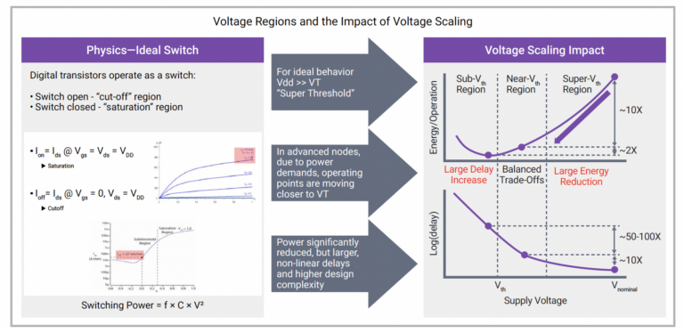
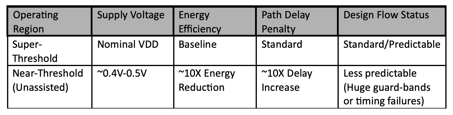
Lowering VDD to near-threshold levels delivers a ~10X reduction in energy per operation. However, because transistor drive currents drop sharply, path delays jump by ~10X. Pushing further toward and below Vth yields only marginal additional energy savings (~2X) while delay surges by ~50X to 100X.
VDD를 근문턱 수준으로 낮추면 연산당 에너지가 약 10배 감소합니다. 그러나 트랜지스터 구동 전류가 급격히 떨어지기 때문에 경로 지연은 약 10배 뛰어오릅니다. 여기서 Vth에 더 가깝게 혹은 그 이하로 밀어붙이면 추가적인 에너지 절감은 미미한 반면(~2배), 지연은 약 50배에서 100배까지 급증합니다.
At near-threshold voltages, timing becomes overwhelmingly dominated by process, voltage, and temperature (PVT) variations and jitter. Small, localized fluctuations in load, slew, or temperature can easily push safe paths into timing failure. Achieving reliable signoff demands waveform-aware timing models, expanded PVT corner sets, and silicon-proven modeling integrity verified at the lowest target supply voltage.
근문턱 전압 영역에서는 타이밍이 공정, 전압, 온도(PVT) 변동과 지터(jitter)에 의해 압도적으로 지배됩니다. 부하, 슬루(slew), 온도에서의 작고 국부적인 변동만으로도 안전한 경로가 쉽게 타이밍 실패로 이어질 수 있습니다. 신뢰할 수 있는 사인오프를 달성하려면 파형 인식(waveform-aware) 타이밍 모델, 확장된 PVT 코너 세트, 그리고 최저 목표 공급 전압에서 검증된 실리콘 인증 모델링 무결성이 요구됩니다.
Restoring Predictability with Low-Voltage Foundation IP
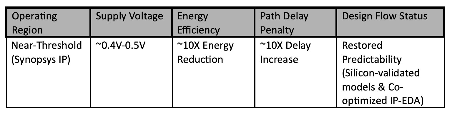
Designing at 0.4V doesn’t mean giving up on a predictable design flow. It requires upgrading the foundation you build on by co-optimizing the underlying Foundation IP stack with EDA signoff tools. Chip architects can reconcile non-linear low-voltage physics with standard implementation tools, restoring design flow predictability at ~0.4V.
0.4V에서의 설계가 예측 가능한 설계 플로우를 포기하는 것을 의미하지는 않습니다. 이는 기반이 되는 파운데이션 IP 스택을 EDA 사인오프 툴과 공동 최적화함으로써 구축하는 기반을 업그레이드해야 함을 뜻합니다. 칩 아키텍트들은 비선형 저전압 물리학을 표준 구현 툴과 조화시켜, 약 0.4V에서 설계 플로우의 예측 가능성을 회복할 수 있습니다.
Low-Voltage Logic Libraries That Understand Variation
Synopsys Logic Libraries utilize moment-based Liberty Variation Format (LVF) characterization and low-voltage-aware models to capture non-linear delay and slew behaviors across wide PVT corners. Coupled with enhanced verification checks for Multiple Input Switching (MIS) effects, skew interactions, and pulse-width integrity, and validated in silicon, this helps ensure signoff models correlate closely with real-world silicon behavior.
시놉시스 로직 라이브러리는 모멘트 기반 라이버티 변동 형식(LVF) 특성화 및 저전압 인식 모델을 활용하여 넓은 PVT 코너 전반에 걸친 비선형 지연 및 슬루 거동을 포착합니다. 다중 입력 스위칭(MIS) 효과, 스큐 상호작용, 펄스 폭 무결성에 대한 향상된 검증 검사와 결합되고 실리콘에서 검증됨으로써, 이는 사인오프 모델이 실제 실리콘 거동과 긴밀하게 상관관계를 갖도록 돕습니다.
Overcoming the Memory Vmin Bottleneck
Memories dominate die area and contribute significantly to power in AI accelerators, and memory Vmin often dictates the SoC’s minimum operating voltage. To overcome this bottleneck, Synopsys provides tailored architectural options:
메모리는 다이 면적을 지배하고 AI 가속기의 전력에 상당 부분 기여하며, 메모리 Vmin은 종종 SoC의 최소 작동 전압을 좌우합니다. 이 병목 현상을 극복하기 위해 시놉시스는 맞춤형 아키텍처 옵션을 제공합니다.
Single-Rail SRAMs with Assist Circuits: Silicon-validated assist features let single-rail macros operate down to typically ~600mV macro Vmin for straightforward V2 energy scaling.
보조 회로가 포함된 싱글레일(Single-Rail) SRAM: 실리콘으로 검증된 보조 기능을 통해 싱글레일 매크로가 V2 에너지 스케일링을 위해 전형적으로 약 600mV 매크로 Vmin까지 내려가 작동할 수 있습니다.
Dual-Rail Memory Architectures: For systems pushing logic toward near-threshold, dual-rail SRAM decouples the logic supply from the memory array supply using robust level shifters. This allows logic to achieve maximum power savings while memory maintains very high density ( 38 Mb/mm² at 380/540mV in 3nm FinFET, as presented at ISSCC 2025) .
듀얼레일(Dual-Rail) 메모리 아키텍처: 로직을 근문턱 영역으로 밀어붙이는 시스템의 경우, 듀얼레일 SRAM은 견고한 레벨 시프터를 사용하여 로직 공급 전압을 메모리 어레이 공급 전압과 분리합니다. 이를 통해 로직은 최대의 전력 절감을 달성하는 동시에 메모리는 매우 높은 밀도(ISSCC 2025에서 발표된 3nm FinFET 공정 기준 38Mb/mm² @ 380/540mV)를 유지할 수 있습니다.
Ultra-Low Power Register Files (ULP RFs): Wide-datapath activation and pooling blocks use ULP RFs running right at the logic Vmin floor to bridge synthesized register arrays and large RF macros.
초저전력 레지스터 파일(ULP RFs): 넓은 데이터패스 활성화 및 풀링 블록은 로직 Vmin 최하단에서 바로 작동하는 ULP RF를 사용하여 합성된 레지스터 어레이와 대형 RF 매크로를 연결합니다.
Low-Voltage Ready I/O
Low-voltage ready I/O libraries help prevent I/O domains from setting system Vmin floors. The portfolio covers control interfaces (GPIO, I3C/I2C, SWI3S), high-speed links (LVDS, RGMII), storage interfaces (SD/eMMC), and 2.5D/3D chiplet I/O.
저전압 준비형 I/O 라이브러리는 I/O 도메인이 시스템 Vmin 최하단을 설정하는 것을 방지하는 데 도움을 줍니다. 이 포트폴리오는 제어 인터페이스(GPIO, I3C/I2C, SWI3S), 고속 링크(LVDS, RGMII), 스토리지 인터페이스(SD/eMMC), 그리고 2.5D/3D 칩릿 I/O를 아우릅니다.
IP-EDA Co-Optimization and Customization
Near-threshold design requires tight co-optimization between cell architectures, compiler settings, and EDA implementation tools.
근문턱 설계는 셀 아키텍처, 컴파일러 설정, 그리고 EDA 구현 툴 간의 긴밀한 공동 최적화를 요구합니다.
When off-the-shelf IP is insufficient for unique SoC constraints, Synopsys provides customer-specific solution fine-tuning alongside Design-Technology Co-Optimization (DTCO) and custom design and characterization services. This can include custom low-voltage logic cells, custom level shifters, tailored dual-rail memory compilers, and specialized PVT signoff corners.
기성(off-the-shelf) IP가 고유한 SoC 제약 조건에 부족할 경우, 시놉시스는 설계-기술 공동 최적화(DTCO) 및 맞춤형 설계·특성화 서비스와 함께 고객 맞춤형 솔루션 미세 조정(fine-tuning)을 제공합니다. 여기에는 맞춤형 저전압 로직 셀, 맞춤형 레벨 시프터, 맞춤형 듀얼레일 메모리 컴파일러, 그리고 특화된 PVT 사인오프 코너가 포함될 수 있습니다.
Silicon Proof: 20% Power Reduction in Production AI Silicon
The practical value of this platform was demonstrated on a production AI-networking SoC manufactured on an advanced process node. The design team deployed a customized low-voltage Foundation IP solution featuring tuned low-voltage logic cells, custom level shifters, a custom dual-rail memory compiler, and targeted near-threshold PVT corners.
이 플랫폼의 실용성은 첨단 공정 노드로 제조된 양산 AI-네트워킹 SoC에서 입증되었습니다. 설계 팀은 튜닝된 저전압 로직 셀, 맞춤형 레벨 시프터, 맞춤형 듀얼레일 메모리 컴파일러, 그리고 타겟팅된 근문턱 PVT 코너를 특징으로 하는 맞춤형 저전압 파운데이션 IP 솔루션을 배포했습니다.
Key Outcomes:
- ~20% Power Reduction compared to the baseline design.
- Zero Schedule Impact: Met area, performance, and all schedule objectives.
- No Re-spins: Avoided costly re-spins and reduced validation overhead.
핵심 성과:
- ~20% 전력 절감: 베이스라인 설계 대비.
- 일정 영향 없음: 면적, 성능, 그리고 모든 일정 목표 충족.
- 재제작(Re-spin) 없음: 비용이 많이 드는 재제작을 회피하고 검증 오버헤드 감소.
Summary
Very-low voltage and near threshold operation (~0.4V–0.5V) is becoming central to competitive Edge-AI SoCs. While 0.4V introduces severe variation and delay jumps, pairing silicon-proven Foundation IP with moment-based LVF characterization, custom fine-tuning, and tight EDA co-optimization makes deep low-voltage operation practical, with predictable convergence and reduced execution risk.
초저전압 및 근문턱 작동(약 0.4V~0.5V)은 경쟁력 있는 엣지 AI SoC의 핵심으로 자리 잡고 있습니다. 0.4V는 심각한 변동성과 지연 급증을 초래하지만, 실리콘으로 검증된 파운데이션 IP를 모멘트 기반 LVF 특성화, 맞춤형 미세 조정, 그리고 긴밀한 EDA 공동 최적화와 결합하면 예측 가능한 수렴성과 감소된 실행 리스크를 바탕으로 깊은 저전압 작동을 실현할 수 있습니다.



