Reimagining 3D IC Design: From Architecture to Signoff
Source: https://semiwiki.com/eda/siemens-eda/375653-reimagining-3d-ic-design-from-architecture-to-signoff/
By Keith Felton, Andras Vass-Varnai and Todd Burkholder, Siemens EDA
The semiconductor industry is undergoing a fundamental transformation. Heterogeneous integration, the practice of combining multiple chiplets and specialized components into a single advanced packaging platform, has emerged as a powerful alternative to traditional monolithic chip design. This shift promises superior performance, improved power efficiency, greater flexibility, and reduced manufacturing costs. Yet realizing these benefits requires a complete reimagining of how semiconductor companies design, verify, and manufacture complex systems.
반도체 산업은 근본적인 전환기를 겪고 있습니다. 여러 개의 칩렛과 특화된 컴포넌트를 단일 첨단 패키징 플랫폼으로 결합하는 이기종 통합(heterogeneous integration)은 전통적인 단일 다이(monolithic) 칩 설계의 강력한 대안으로 부상했습니다. 이 전환은 우수한 성능, 향상된 전력 효율, 더 큰 유연성, 그리고 제조 비용 절감을 약속합니다. 하지만 이러한 이점을 실현하려면 반도체 기업이 복잡한 시스템을 설계, 검증, 제조하는 방식을 완전히 새롭게 재상상해야 합니다.
Siemens Innovator3D IC™ product family addresses this challenge with a unified design platform that spans the entire product lifecycle, from early architectural exploration through final manufacturing signoff. Rather than relying on disconnected point tools that force teams to work in silos, the platform creates a continuous digital thread connecting silicon designers, package architects, verification engineers, and reliability specialists around a common 3D digital twin.
지멘스의 Innovator3D IC™ 제품군은 초기 아키텍처 탐색부터 최종 제조 승인(signoff)에 이르기까지 전체 제품 수명 주기를 아우르는 통합 설계 플랫폼으로 이 문제에 대응합니다. 팀들이 사일로(silo) 형태로 고립되어 일하도록 강제하는 단절된 개별 툴에 의존하는 대신, 이 플랫폼은 공통된 3D 디지털 트윈을 중심으로 실리콘 디자이너, 패키지 아키텍트, 검증 엔지니어, 신뢰성 전문가를 연결하는 연속적인 디지털 스레드(digital thread)를 생성합니다.
The Case for Heterogeneous Integration
The traditional approach to semiconductor design centered on monolithic architectures, where all functionality resided on a single die. This model worked well for decades, but it increasingly struggles to meet the silicon scaling demands of artificial intelligence, hyperscale computing, and high-performance applications. These workloads require combinations of specialized processors, high-bandwidth memory, and custom accelerators that are difficult to integrate efficiently on a single piece of silicon due to reticle size limits and yield challenges.
전통적인 반도체 설계 접근 방식은 모든 기능이 단일 다이에 존재하는 단일체(monolithic) 아키텍처를 중심으로 이루어졌습니다. 이 모델은 수십 년 동안 잘 작동했지만, 인공지능(AI), 하이퍼스케일 컴퓨팅, 고성능 애플리케이션의 실리콘 스케일링 요구 사항을 충족하는 데 점점 더 어려움을 겪고 있습니다. 이러한 워크로드는 특화된 프로세서, 고대역폭 메모리, 커스텀 가속기의 조합을 필요로 하지만, 레티클(reticle) 크기 한계와 수율 문제로 인해 단일 실리콘 조각 위에 효율적으로 통합하기가 어렵습니다.
Heterogeneous integration solves this problem by allowing engineers to assemble pre-designed, custom, or third-party chiplets onto high-performance interposers and advanced package substrates. This modular approach enables companies to mix and match components optimized for specific functions, rather than forcing all logic into a single die at a single process node. The results are systems that deliver better performance per watt, scale more flexibly as requirements change, and cost less to manufacture at volume.
이기종 통합은 엔지니어들이 미리 설계된 커스텀 또는 타사 칩렛을 고성능 인터포저(interposer) 및 첨단 패키지 기판 위에 조립할 수 있도록 함으로써 이 문제를 해결합니다. 이 모듈식 접근 방식을 통해 기업들은 모든 로직을 단일 공정 노드의 단일 다이에 강제로 우겨넣는 대신, 특정 기능에 최적화된 컴포넌트들을 조합(mix-and-match)할 수 있습니다. 그 결과 와트당 더 나은 성능을 제공하고, 요구 사항 변화에 따라 더 유연하게 확장되며, 대량 생산 시 제조 비용이 절감되는 시스템이 탄생합니다.
However, existing design tools were built for single-die devices and cannot adequately handle the complexity of 2.5D and 3D IC designs. A new methodology is required, one that takes a system-centric view from initial planning through final sign-off. This is where the Innovator3D IC product family enters the picture.
그러나 기존의 섭외 설계 툴은 단일 다이 디바이스용으로 제작되었기 때문에 2.5D 및 3D IC 설계의 복잡성을 적절히 처리할 수 없습니다. 초기 계획 단계부터 최종 승인까지 시스템 중심의 관점을 취하는 새로운 방법론이 필요하며, 여기서 Innovator3D IC 제품군이 등장하게 됩니다.
Building the Digital Twin Foundation
At the heart of the Innovator3D IC platform is the 3D digital twin, a comprehensive virtual representation of the entire device assembly. Creating this twin begins with aggregating design data from multiple sources to construct a full-system model. This model drives the creation of interfaces and bump arrays for chiplets, bridges, interposers, and substrates, resulting in a single authoritative source of system connectivity.
Innovator3D IC 플랫폼의 핵심은 전체 디바이스 어셈블리의 포괄적인 가상 표현인 3D 디지털 트윈입니다. 이 트윈을 구축하는 것은 여러 소스의 설계 데이터를 집계하여 전체 시스템 모델을 구성하는 것부터 시작합니다. 이 모델은 칩렛, 브리지, 인터포저, 기판을 위한 인터페이스 및 범프(bump) 어레이의 생성을 주도하여 단일한 공인 시스템 연결 소스를 만들어냅니다.
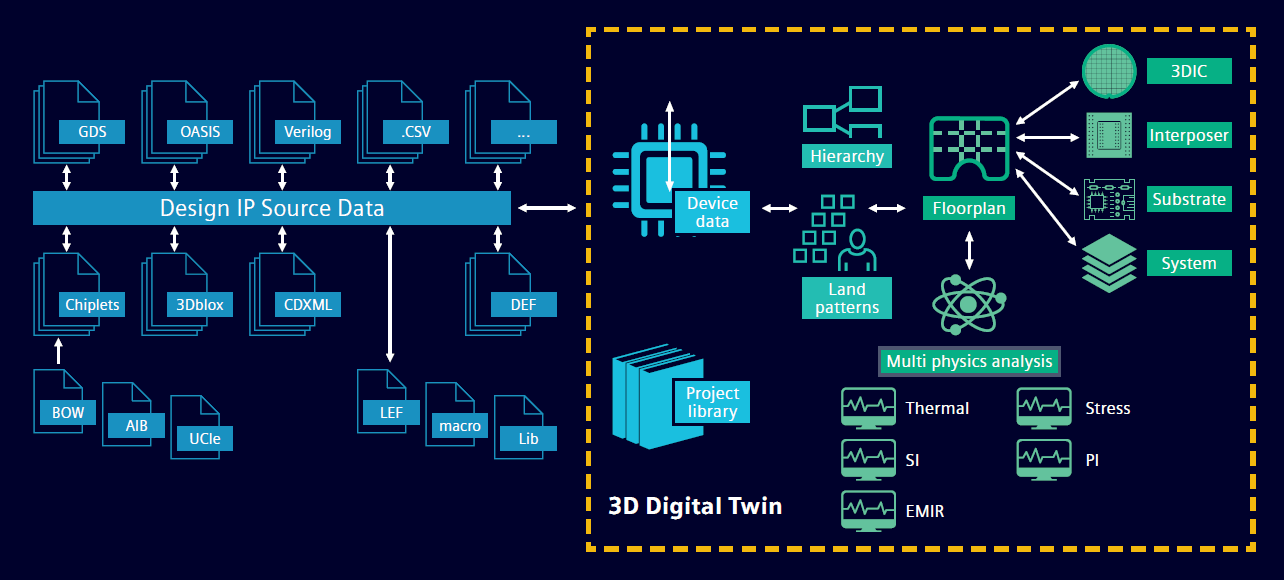
This task is more complex than it sounds. Heterogeneous designs can contain over 50 million total pins and hundreds of thousands of connections. Traditional spreadsheet-based approaches, once adequate for smaller designs, become error-prone and unmanageable at this scale. The industry is developing standardized data formats, such as IEEE 3Dblox, OCP CDX, and JEDEC JEP30 Part Model, to simplify integration and improve interoperability. These standards promote compatibility between chiplets and streamline the exchange of comprehensive component information.
이 작업은 들리는 것보다 훨씬 복잡합니다. 이기종 설계는 총 5천만 개 이상의 핀과 수십만 개의 연결을 포함할 수 있습니다. 과거 소규모 설계에는 적절했던 전통적인 스프레드시트 기반 접근 방식은 이 규모에서는 오류가 발생하기 쉽고 관리 불가능해집니다. 업계는 통합을 단순화하고 상호 운용성을 향상시키기 위해 IEEE 3Dblox, OCP CDX, JEDEC JEP30 파트 모델과 같은 표준화된 데이터 포맷을 개발하고 있습니다. 이러한 표준은 칩렛 간의 호환성을 촉진하고 포괄적인 컴포넌트 정보 교환을 간소화합니다.
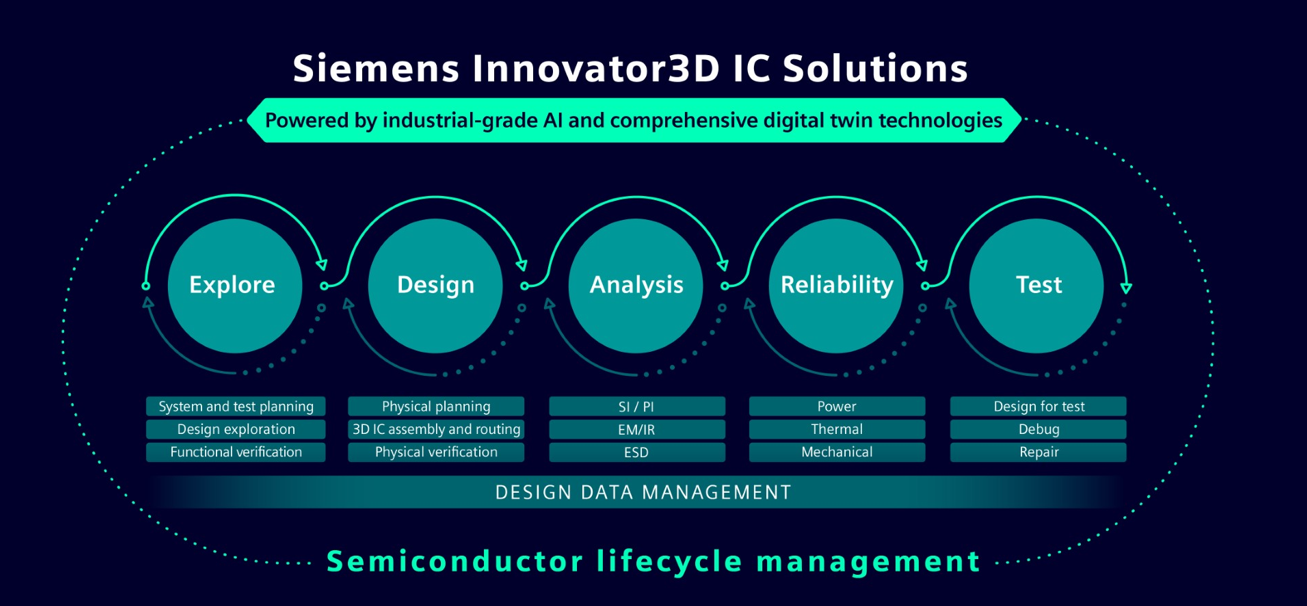
The digital twin serves as the foundation linking every stage of development. It enables true system-level technology co-optimization (STCO) across silicon, interposers, package substrates, and system PCBs. Because all teams reference the same digital representation throughout the design process, design intent remains consistent and integration surprises are minimized. Innovator3D IC Integrator supports this concept with a comprehensive design cockpit spanning the explore, design, analysis, reliability, and test domains.
디지털 트윈은 개발의 모든 단계를 연결하는 기반 역할을 합니다. 이를 통해 실리콘, 인터포저, 패키지 기판, 시스템 PCB 전반에 걸쳐 진정한 시스템 수준 기술 공동 최적화(STCO, System-level Technology Co-Optimization)가 가능합니다. 모든 팀이 설계 프로세스 내내 동일한 디지털 표현을 참조하기 때문에 설계 의도가 일관되게 유지되고 통합 상항의 충격이 최소화됩니다. Innovator3D IC Integrator는 탐색, 설계, 분석, 신뢰성, 테스트 도메인을 아우르는 포괄적인 설계 콕핏(cockpit)으로 이 개념을 지원합니다.
Explore: Architectural Options
Before implementation begins, architects must determine which integration strategy best satisfies power, performance, area, cost, quality, manufacturability, and test objectives. The “Explore” domain within Innovator3D IC Integrator enables silicon designers, package architects, and system designers to collaborate on early planning and feasibility analysis using a common digital twin.
구현이 시작되기 전에 아키텍트는 전력, 성능, 면적, 비용, 품질, 제조 용이성 및 테스트 목표를 가장 잘 충족하는 통합 전략이 무엇인지 결정해야 합니다. Innovator3D IC Integrator 내의 '탐색(Explore)' 도메인을 통해 실리콘 디자이너, 패키지 아키텍트, 시스템 디자이너는 공통 디지털 트윈을 사용하여 초기 계획 및 타당성 분석에 대해 협업할 수 있습니다.
Leveraging predictive modeling and machine learning-assisted design-space exploration, engineering teams can evaluate multiple system-in-package scenarios before committing resources to physical implementation. These evaluations include chiplet partitioning studies, package technology comparisons, floorplanning assessments, routability analyses, power delivery investigations, thermal feasibility studies, signal integrity assessments, and test planning activities.
예측 모델링과 머신러닝 기반 설계 공간 탐색을 활용하여 엔지니어링 팀은 물리적 구현에 자원을 투입하기 전에 여러 시스템인패키지(SiP) 시나리오를 평가할 수 있습니다. 이러한 평가에는 칩렛 파티셔닝 연구, 패키지 기술 비교, 플로어플래닝 평가, 라우팅 가능성 분석, 전력 공급 조사, 열 타당성 연구, 신호 무결성 평가, 테스트 계획 활동이 포함됩니다.
The key advantage is that all these activities occur using the same digital twin that will ultimately drive implementation and sign-off. This continuity ensures that design intent established during exploration carries through to the final product, reducing downstream rework and accelerating convergence toward an optimal solution.
핵심적인 장점은 이러한 모든 활동이 궁극적으로 구현과 승인을 주도할 동일한 디지털 트윈을 사용하여 수행된다는 점입니다. 이러한 연속성은 탐색 단계에서 수립된 숲이 최종 제품까지 이어지도록 보장하여 다운스트림 재작업을 줄이고 최적의 솔루션을 향한 수렴을 가속화합니다.
Design: Implementing the Selected Architecture
Once an optimal architecture has been identified, the focus shifts to physical implementation. The “Design” domain provides a unified environment for chiplet, interposer, and advanced package implementation. This stage requires translating system intent into a manufacturable multi-die design while preserving the connectivity, performance, and reliability objectives established earlier.
최적의 아키텍처가 확인되면 초점은 물리적 구현으로 전환됩니다. '설계(Design)' 도메인은 칩렛, 인터포저, 첨단 패키지 구현을 위한 통합 환경을 제공합니다. 이 단계에서는 이전에 설정된 연결성, 성능, 신뢰성 목표를 보존하면서 시스템 의도를 제조 가능한 멀티 다이 설계로 변환해야 합니다.
The implementation process begins with interface and bump array construction. Many package designs exhibit repeatable patterns that can be represented as parameterized objects. Rather than modeling each device as a flat entity, designers can represent them as hierarchical building blocks with topological pin regions defined using formulas, regular expressions, and design attribute tokens. This approach dramatically accelerates design creation and enables rapid iteration.
구현 프로세스는 인터페이스 및 범프 어레이 구축으로 시작됩니다. 많은 패키지 설계는 매개변수화된 객체로 표현할 수 있는 반복 가능한 패턴을 보여줍니다. 각 디바이스를 단일체 엔티티로 모델링하는 대신, 디자이너는 공식, 정규식, 설계 속성 토큰을 사용하여 정의된 위상학적 핀 영역을 가진 계층적 빌딩 블록으로 표현할 수 있습니다. 이 접근 방식은 설계 생성을 극적으로 가속화하고 빠른 반복을 가능하게 합니다.
System-level netlist creation and validation represents another critical step. With designs containing millions of connections, language-based design approaches using Verilog RTL and proper bus notation prove far more efficient and reliable than bit-by-bit spreadsheet definitions. This enables designers to manage the explosion of die-to-die connections while ensuring that interface definitions, bump assignments, and connectivity remain synchronized as development progresses.
시스템 수준 넷리스트(netlist) 생성 및 검증은 또 다른 중요한 단계입니다. 수백만 개의 연결을 포함하는 설계의 경우, Verilog RTL 및 적절한 버스 표기법을 사용하는 언어 기반 설계 접근 방식이 비트 단위의 스프레드시트 정의보다 훨씬 더 효율적이고 신뢰할 수 있음이 입증되었습니다. 이를 통해 디자이너는 다이 간 연결의 폭증을 관리하는 동시에 개발이 진행됨에 따라 인터페이스 정의, 범프 할당, 연결성이 동기화된 상태를 유지하도록 보장할 수 있습니다.
Bridge and interposer instantiation follows naturally from connectivity. Rather than designing these components from scratch, the most efficient approach derives them as functions of the devices they interconnect, leveraging the already-verified netlist. Innovator3D IC Integrator uniquely represents the entire system within a single environment, from early hierarchical device planning through final sign-off.
브리지 및 인터포저 인스턴스화(instantiation)는 연결성으로부터 자연스럽게 도출됩니다. 이러한 컴포넌트를 처음부터 새로 설계하는 대신, 이미 검증된 넷리스트를 활용하여 상호 연결하는 디바이스의 함수로 파생하는 것이 가장 효율적인 접근 방식입니다. Innovator3D IC Integrator는 초기 계층적 디바이스 계획부터 최종 승인에 이르기까지 단일 환경 내에서 전체 시스템을 고유하게 표현합니다.
Logic and memory devices require high-speed, high-bandwidth interfaces, necessitating close proximity often achieved through silicon bridge devices. Most multi-device packages also require substrate stiffeners, seal rings, thermal interface materials, and heat spreaders for thermal management and encapsulation. These mechanical objects occupy real estate and require clearance considerations, directly impacting placement strategies.
로직 및 메모리 디바이스는 고속, 고대역폭 인터페이스를 필요로 하며, 이는 실리콘 브리지 디바이스를 통해 자주 달성되는 근접성을 요구합니다. 대부분의 멀티 디바이스 패키지는 또한 열 관리 및 밀봉을 위해 기판 스티프너(stiffener), 실 링(seal ring), 열 인터페이스 재료, 히트 스프레더를 필요로 합니다. 이러한 기계적 객체는 공간을 차지하며 간섭 고려 사항이 필요하므로 배치 전략에 직접적인 영향을 미칩니다.
Connectivity planning across substrate boundaries typically focuses on high-performance die-to-die interfaces and die-to-package connections. Enabling effective STCO requires new levels of intelligence in design tools. Innovator3D IC Integrator employs machine learning algorithms to concurrently optimize connectivity and device pin and bump assignments across all hierarchy levels, balancing resources across all domains to achieve high-performance, cost-effective solutions in the shortest time.
기판 경계를 가로지르는 연결성 계획은 일반적으로 고성능 다이 간 인터페이스와 다이 대 패키지 연결에 초점을 맞춥니다. 효과적인 STCO(시스템 수준 기술 공동 최적화)를 가능하게 하려면 설계 툴에 새로운 수준의 지능이 필요합니다. Innovator3D IC Integrator는 머신러닝 알고리즘을 사용하여 모든 계층 수준에서 연결성과 디바이스 핀 및 범프 할당을 동시에 최적화하며, 모든 도메인의 리소스 균형을 맞춰 가장 짧은 시간에 고성능의 비용 효율적인 솔루션을 달성합니다.
Power delivery network (PDN) prototyping and predictive analysis follow connectivity optimization. Increased power and performance demands in semiconductor packages have escalated power delivery challenges, making early analysis critical. Designers must prototype PDNs to provide sufficient and stable power while managing spatial constraints in dense designs. After prototyping, designers analyze the PDN for suitability, identifying significant DC-drop issues early to prevent costly changes. Once DC-drop requirements are met, the focus shifts to metal density across each layer, with automatic addition of user-defined metal areas to balance layers and prevent substrate warpage.
전력 공급 네트워크(PDN) 프로토타이핑 및 예측 분석은 연결성 최적화에 뒤이어 진행됩니다. 반도체 패키지의 전력 및 성능 요구 사항 증가로 인해 전력 공급 과제가 고조되었으며, 이로 인해 조기 분석이 매우 중요해졌습니다. 디자이너는 조밀한 설계에서 공간적 제약을 관리하는 동시에 충분하고 안정적인 전력을 제공하기 위해 PDN을 프로토타이핑해야 합니다. 프로토타이핑 후 디자이너는 적합성에 대해 PDN을 분석하여 중요한 DC 드롭 문제를 조기에 파악하고 비용이 많이 드는 변경을 방지합니다. DC 드롭 요구 사항이 충족되면 초점은 각 레이어의 금속 밀도로 이동하며, 레이어의 균형을 맞추고 기판 휨을 방지하기 위해 사용자가 정의한 금속 영역을 자동으로 추가합니다.
Analysis: Multiphysics Verification
As heterogeneous systems grow in complexity, traditional point-tool analysis methodologies struggle to capture interactions between silicon, interposers, bridge dies, redistribution layers, and advanced package structures. Innovator3D IC Integrator extends beyond physical planning by providing a unified analysis framework operating directly from the digital twin.
이기종 시스템의 복잡성이 증가함에 따라 전통적인 개별 툴 분석 방법론은 실리콘, 인터포저, 브리지 다이, 재배선 레이어(RDL), 첨단 패키지 구조 간의 상호 작용을 포착하는 데 어려움을 겪습니다. Innovator3D IC Integrator는 디지털 트윈에서 직접 작동하는 통합 분석 프레임워크를 제공하여 물리적 계획을 넘어 확장됩니다.
The “Analysis” domain supports end-to-end electrical and mechanical verification across the complete assembly, enabling signal integrity, power integrity, and IR-drop as well as thermal and thermo-mechanical evaluation from early architectural studies through final sign-off. Engineers can analyze full or partial implementations using intermediate package databases long before final design completion, identifying potential bottlenecks, voltage droop concerns, routing limitations, channel degradation issues, and reliability concerns while architectural changes remain relatively inexpensive.
'분석(Analysis)' 도메인은 전체 어셈블리에 걸쳐 엔드투엔드 전기 및 기계적 검증을 지원하며, 초기 연구부터 최종 승인에 이르기까지 신호 무결성(SI), 전력 무결성(PI), IR 드롭뿐만 아니라 열 및 열-기계적 평가를 가능하게 합니다. 엔지니어는 최종 설계 완료 시점보다 훨씬 이전에 중간 패키지 데이터베이스를 사용하여 전체 또는 부분 구현을 분석할 수 있으며, 아키텍처 변경이 상대적으로 비용이 저렴한 시점에 잠재적인 병목 현상, 전압 강하 우려, 라우팅 제한, 채널 저하 문제, 신뢰성 우려를 파악할 수 있습니다.
By combining technologies such as HyperLynx™, mPower™, and advanced extraction solutions within a common workflow, engineers gain continuous visibility into electrical performance across all design domains. Automated testbench creation and coordinated multidomain analysis help shorten design cycles while improving confidence in sign-off readiness.
공통 워크플로우 내에서 HyperLynx™, mPower™ 및 고급 추출 솔루션과 같은 기술을 결합함으로써 엔지니어는 모든 설계 도메인에 걸쳐 전기적 성능에 대한 지속적인 가시성을 확보할 수 있습니다. 자동화된 테스트벤치 생성과 조율된 멀티도메인 분석은 설계 주기를 단축하는 동시에 승인 준비 상태에 대한 신뢰도를 향상시킵니다.
Modern advanced packages must also meet stringent thermal, mechanical, and long-term reliability requirements. Historically, thermal and thermo-mechanical analysis occurred after substantial design completion, introducing significant risk because package architecture decisions directly influence thermal behavior, warpage, stress distribution, and long-term reliability.
현대 첨단 패키지는 또한 엄격한 열, 기계적, 장기 신뢰성 요구 사항을 충족해야 합니다. 역사적으로 열 및 열-기계적 분석은 상당한 설계가 완료된 후에 이루어졌으며, 패키지 아키텍처 결정이 열 거동, 휨, 응력 분포, 장기 신뢰성에 직접적인 영향을 미치기 때문에 상당한 위험을 초래했습니다.
Innovator3D IC product family integrates thermal and mechanical verification directly into the design cockpit, enabling architects and package designers to initiate and evaluate multiphysics simulations throughout development. Through integration with Calibre® 3DThermal, Calibre 3DStress, Simcenter™ Flotherm, and Simcenter Simlab, users can assess thermal performance, package warpage, mechanical stress, vibration effects, and manufacturing-induced stresses across the entire assembly.
Innovator3D IC 제품군은 열 및 기계적 검증을 설계 콕핏에 직접 통합하여 아키텍트와 패키지 디자이너가 개발 과정 전반에 걸쳐 멀티피직스 시뮬레이션을 시작하고 평가할 수 있도록 합니다. Calibre® 3DThermal, Calibre 3DStress, Simcenter™ Flotherm, Simcenter Simlab과의 통합을 통해 사용자는 전체 어셈블리에 걸쳐 열 성능, 패키지 휨, 기계적 응력, 진동 효과, 제조 유발 응력을 평가할 수 있습니다.
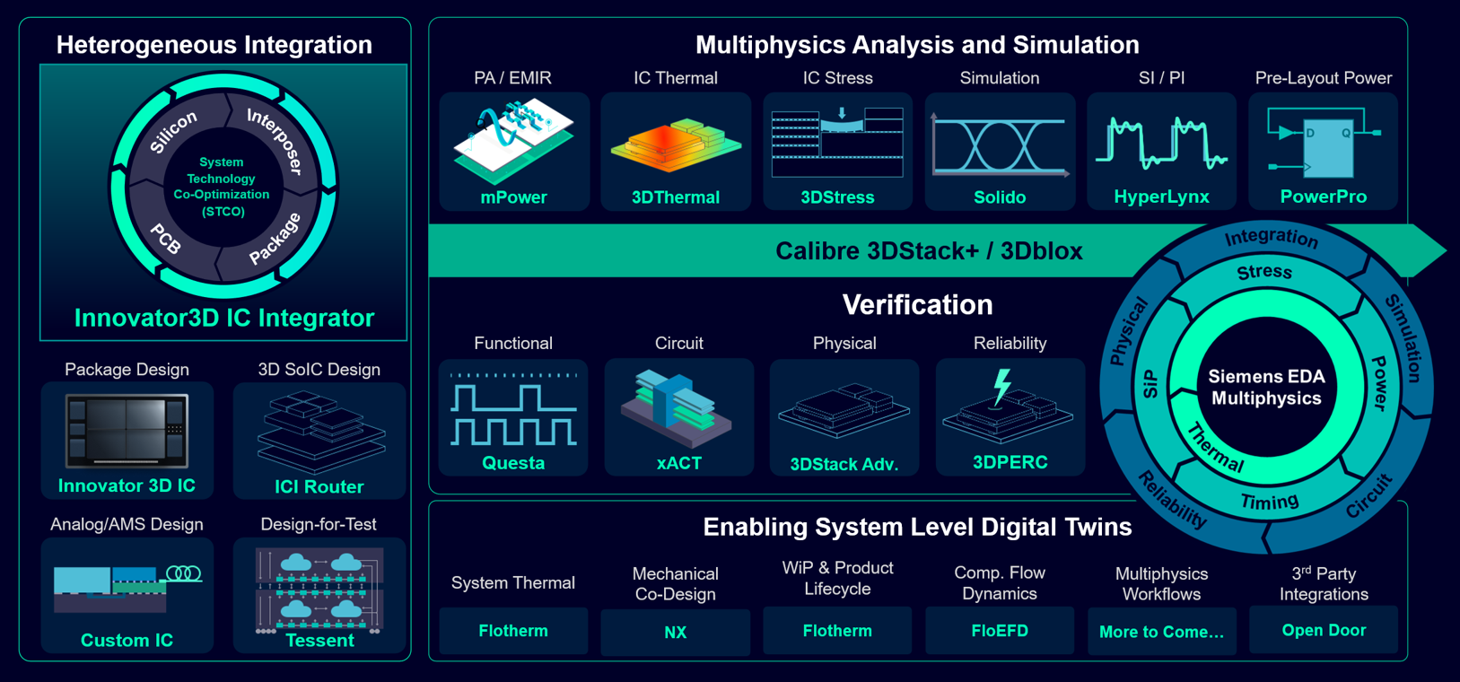
Because reliability analysis connects to the same digital twin used for planning and implementation, teams can evaluate design tradeoffs earlier and establish a common digital thread extending from architecture exploration through manufacturing sign-off. The shared digital twin allows package architects, silicon teams, and reliability specialists to evaluate tradeoffs using a unified representation of the system.
신뢰성 분석은 계획 및 구현에 사용되는 동일한 디지털 트윈에 연결되므로, 팀은 설계 절충안을 더 일찍 평가하고 아키텍처 탐색부터 제조 승인까지 확장되는 공통 디지털 스레드를 구축할 수 있습니다. 공유된 디지털 트윈을 통해 패키지 아키텍트, 실리콘 팀, 신뢰성 전문가는 시스템의 통합된 표현을 사용하여 절충안을 평가할 수 있습니다.
Test: Planning for Manufacturability and Yield
Complex multi-die assemblies must be optimized for manufacturing test, debug, repair, and long-term yield. The “Test” domain of Innovator3D IC leverages IEEE 1838-based multi-die test methodologies together with thermal-aware test planning to ensure that high-activity test patterns do not introduce excessive power or thermal stress during manufacturing. By connecting DFT planning, thermal analysis, and validation within the same digital twin environment, engineering teams can improve fault coverage, accelerate test development, and reduce the risk of yield loss and latent reliability issues.
복잡한 멀티 다이 어셈블리는 제조 테스트, 디버그, 수리, 장기 수율을 위해 최적화되어야 합니다. Innovator3D IC의 '테스트(Test)' 도메인은 IEEE 1838 기반 멀티 다이 테스트 방법론을 열 인식 테스트 계획과 결합하여 고활동 테스트 패턴이 제조 중에 과도한 전력이나 열 응력을 유발하지 않도록 보장합니다. DFT 계획, 열 분석, 검증을 동일한 디지털 트윈 환경 내에서 연결함으로써 엔지니어링 팀은 결함 커버리지를 향상시키고, 테스트 개발을 가속화하며, 수율 손실 및 잠재적 신뢰성 문제의 위험을 줄일 수 있습니다.
Accelerating Time to Market
The future of heterogeneous integration requires a design methodology extending far beyond physical implementation. Engineering organizations need a platform capable of supporting architectural exploration, digital-twin creation, physical implementation, multiphysics verification, reliability assessment, and sign-off within a unified environment.
이기종 통합의 미래는 물리적 구현을 훨씬 뛰어넘는 설계 방법론을 요구합니다. 엔지니어링 조직은 통합된 환경 내에서 아키텍처 탐색, 디지털 트윈 구축, 물리적 구현, 멀티피직스 검증, 신뢰성 평가, 승인을 지원할 수 있는 플랫폼이 필요합니다.
Innovator3D IC Integrator delivers this capability through a comprehensive design cockpit spanning Explore, Design, Analysis, Reliability, and Test domains. Using a common 3D digital twin and continuous digital thread, teams can evaluate architectural alternatives, optimize connectivity, perform predictive multiphysics analysis, assess product reliability, and validate design readiness long before manufacturing.
Innovator3D IC Integrator는 탐색, 설계, 분석, 신뢰성, 테스트 도메인을 아우르는 포괄적인 설계 콕핏을 통해 이 능력을 제공합니다. 공통 3D 디지털 트윈과 연속적인 디지털 스레드를 사용하여 팀은 제조 이전에 아키텍처 대안을 평가하고, 연결성을 최적화하고, 예측 멀티피직스 분석을 수행하고, 제품 신뢰성을 평가하고, 설계 준비 상태를 검증할 수 있습니다.
By unifying traditionally disconnected workflows and enabling STCO, Innovator3D IC Integrator helps design teams reduce iterations, improve predictability, and accelerate time-to-market. The platform allows engineering organizations to confidently deliver the next generation of advanced heterogeneous systems by maintaining a single source of truth throughout the entire design lifecycle. In an industry where time-to-market directly translates to competitive advantage, this unified approach represents a fundamental shift in how complex semiconductor systems are developed.
전통적으로 단절된 워크플로우를 통합하고 STCO를 가능하게 함으로써 Innovator3D IC Integrator는 설계 팀이 반복 작업을 줄이고, 예측 가능성을 향상시키며, 출시 기간을 단축할 수 있도록 돕습니다. 이 플랫폼을 통해 엔지니어링 조직은 전체 설계 수명 주기 동안 단일 진실 공급원(Single Source of Truth)을 유지함으로써 차세대 첨단 이기종 시스템을 자신 있게 선보일 수 있습니다. 출시 기간이 곧 경쟁 우위로 직결되는 산업에서 이 통합된 접근 방식은 복잡한 반도체 시스템이 개발되는 방식을 바꾸는 근본적인 변화를 의미합니다.
To learn more on how to improve your 3D IC flow, please check out the new whitepapers from Siemens: From architecture exploration to signoff: Accelerating the 3D IC lifecycle and Reliability in 3D IC design: A proactive multi-physics approach.
3D IC 플로우를 개선하는 방법에 대해 자세히 알아보려면 지멘스의 새로운 백서들을 확인해 보세요: 《아키텍처 탐색부터 승인까지: 3D IC 수명 주기 가속화(From architecture exploration to signoff: Accelerating the 3D IC lifecycle)》 및 《3D IC 설계의 신뢰성: 사전 예방적 멀티피직스 접근 방식(Reliability in 3D IC design: A proactive multi-physics approach)》.
Keith Felton is the Principle Technical Product Marketing Manager for the Innovator3D IC product family at Siemens DISW in Marlborough, MA. Working extensively in IC package design since the late 1980s, Keith drove the launch of the industry’s first dedicated system-in-package design solution in the early 2000s and led the team that launched Siemens OSAT Alliance program. His current focus includes driving the strategy and direction for Siemens multi-substrate prototyping, design, and verification solution for high-density advanced packaging.
키스 펠튼(Keith Felton): 미국 매사추세츠주 말버러에 위치한 지멘스 DISW의 Innovator3D IC 제품군 수석 테크니컬 제품 마케팅 매니저입니다. 1980년대 후반부터 IC 패키지 설계에 광범위하게 종사해 왔으며, 2000년대 초반 업계 최초의 전용 시스템인패키지(SiP) 설계 솔루션의 출격을 주도했고, 지멘스 OSAT 얼라이언스 프로그램을 출범시킨 팀을 이끌었습니다. 현재 고밀도 첨단 패키징을 위한 지멘스 멀티 서브스트레이트 프로토타이핑, 설계, 검증 솔루션의 전략과 방향을 이끄는 업무에 주력하고 있습니다.
Andras Vass-Varnai is a 3D IC reliability solution engineer at Siemens EDA. Andras is dedicated to contributing to the development of a novel 3D IC package toolchain, leveraging his experience in thermal and reliability engineering. His main areas of interest include thermal management of electronic systems, advanced applications of thermal transient testing and modeling, semiconductor packaging, characterization of TIM materials, and reliability testing of semiconductor devices. Andras Vass-Varnai obtained his MSc and PhD degrees in Electrical Engineering from the Budapest University of Technology and Economics.
안드라스 바스바르나이(Andras Vass-Varnai): 지멘스 EDA의 3D IC 신뢰성 솔루션 엔지니어입니다. 열 및 신뢰성 엔지니어링 분야의 경험을 바탕으로 참신한 3D IC 패키지 툴체인 개발에 기여하고 있습니다. 주요 관심 분야는 전자 시스템의 열 관리, 열 과도 테스트 및 모델링의 첨단 응용, 반도체 패키징, TIM 재료 특성화, 반도체 디바이스의 신뢰성 테스트입니다. 부다페스트 기술경제대학교에서 전기전자공학 석사 및 박사 학위를 취득했습니다.
Todd Burkholder is a Senior Editor at Siemens DISW. For over 25 years, he has worked as editor, author, and ghost writer with internal and external customers to create print and digital content across a broad range of EDA technologies. Todd began his career in marketing for high-technology and other industries in 1992 after earning a Bachelor of Science at Portland State University and a Master of Science degree from the University of Arizona.
토드 버크홀더(Todd Burkholder): 지멘스 DISW의 선임 편집자입니다. 25년 이상 내부 및 외부 고객과 함께 편집자, 저자, 대필 작가로 활동하며 광범위한 EDA 기술 전반에 걸쳐 인쇄 및 디지털 콘텐츠를 제작해 왔습니다. 포틀랜드 주립대학교에서 이학사 학위를, 애리조나 대학교에서 석사 학위를 취득한 후 1992년 하이테크 및 기타 산업 마케팅 분야에서 커리어를 시작했습니다.



