SEMICON West 2026: After the Toast, the Hard Questions
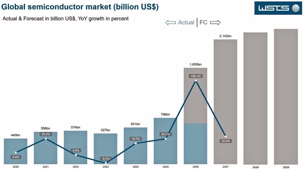
Champagne is an unusual opening act for a semiconductor conference. At SEMICON West 2026, October 13 to 15, at the Moscone Center in San Francisco, it served a purpose. The toast marked an industry that has already crossed $1 trillion in annual revenue, almost four years ahead of earlier projections.
반도체 컨퍼런스에서 샴페인은 다소 이례적인 오프닝 행사입니다. 하지만 지난 10월 13일부터 15일까지 샌프란시스코 모스콘 센터(Moscone Center)에서 열린 'SEMICON West 2026'에서 샴페인은 분명한 목적을 가지고 있었습니다. 이 축배는 당초 예상보다 거의 4년이나 앞서 연간 매출 1조 달러(약 1,300조 원) 고지에 오른 반도체 산업의 성취를 기념하기 위한 것이었습니다.
WSTS (World Semiconductor Trade Statistics) put first-half 2026 sales at $702 billion, double a year earlier, and its August update points to roughly $1.66 trillion for the full year, with memory up about 300%. SEMI chose its theme to match: the road from one trillion to two.
WSTS(세계반도체시장통계기구)는 2026년 상반기 매출을 전년 동기 대비 두 배 증가한 702억 달러로 집계했으며, 8월 수정 전망을 통해 연간 전체 매출이 약 1조 6,600억 달러에 이를 것으로 내다봤습니다. 특히 메모리 반도체는 약 300% 급증할 것으로 예상됩니다. 이에 발맞추어 SEMI(국제반도체장비재료협회)는 이번 행사의 주제를 '1조 달러에서 2조 달러로 향하는 여정(the road from one trillion to two)'으로 정했습니다.
By the numbers
SEMI expected more than 35,000 attendees over the three days on a sold-out floor of over 1,500 booths. Final attendance had not been released when this was written. By SEMI’s own figure, the exhibitor count is more than 700 companies and organizations, covering the whole microelectronic supply chain, from EDA and IP, fabless designers and the big IDMs to equipment and materials.
SEMI는 3일간 매진을 기록한 1,500개 이상의 부스 전시장에 35,000명 이상의 참관객이 방문할 것으로 예상했습니다. 기사 작성 시점에는 최종 참석자 수가 공식 발표되지 않았습니다. SEMI의 자체 집계에 따르면, 참가 기업 및 기관은 EDA(전자 설계 자동화) 및 IP, 팹리스 설계 기업, 대형 IDM(종합반도체기업)부터 장비 및 소재 기업에 이르기까지 마이크로 일렉트로닉 공급망 전체를 아우르는 700여 곳에 달했습니다.
Four topics ran through almost every room: AI scaling, heterogeneous integration, advanced manufacturing and supply-chain resilience. Behind them sat an enviable problem. Demand is extraordinary; the hard part is meeting it within the limits of power, cost and production readiness.
거의 모든 세션에서는 다음 네 가지 주제가 핵심으로 다뤄졌습니다. ▲인공지능(AI) 확장, ▲이종 통합(Heterogeneous Integration), ▲첨단 제조, ▲공급망 탄력성입니다. 그 이면에는 부러움을 살 만한 과제가 자리 잡고 있었습니다. 수요는 폭발적인데, 전력·비용·생산 준비성의 한계 내에서 이를 충족하는 것이 어려운 과제이기 때문입니다.
The CEO Summit stage
Each morning (8:30 to 11) ran under its own banner: “Semiconductors Today” on Tuesday, “Transform Tomorrow” on Wednesday and “Meeting the Industry’s Needs” on Thursday.
매일 오전(8시 30분~11시)에는 각기 다른 주제로 세션이 진행되었습니다.
- 화요일: "오늘의 반도체(Semiconductors Today)"
- 수요일: "내일의 변혁(Transform Tomorrow)"
- 목요일: "산업의 요구 충족(Meeting the Industry’s Needs)"
The session I had circled was Sassine Ghazi’s fireside chat with Ed Sperling of Semiconductor Engineering. The Synopsys CEO described how the company has embedded agentic AI across its entire, very large product portfolio. Few EDA leaders have been this explicit about where the design flow is going. It also raised a question well beyond EDA: what happens when AI takes a growing role in designing the hardware it runs on? Speed is the easy part to demonstrate. Proving that the silicon comes out right is harder.
제가 가장 주목했던 세션은 시놉시스(Synopsys)의 사신 가지(Sassine Ghazi) CEO와 'Semiconductor Engineering'의 에드 스펄링(Ed Sperling) 간의 대담이었습니다. 시놉시스 CEO는 자사가 매우 방대한 전체 제품 포트폴리오 전반에 걸쳐 에이전틱 AI(Agentic AI)를 어떻게 내장했는지 설명했습니다. 디자인 플로우가 나아갈 방향에 대해 이처럼 명시적으로 밝힌 EDA 리더는 드뭅니다. 이는 또한 EDA 분야를 넘어선 중대한 질문을 던졌습니다. 바로 AI가 자기가 구동될 하드웨어를 설계하는 데 점점 더 큰 역할을 맡게 될 때 무슨 일이 벌어질 것인가 하는 점입니다. 속도를 증명하는 것은 쉽습니다. 하지만 실리콘 칩이 제대로 설계되어 나오는지 증명하는 것은 훨씬 더 어려운 일입니다.
Other sessions worth the early start:
- Lalitha Immaneni (VP, Semiconductor R&D, Intel Foundry) on the system era and scaling AI through heterogeneous integration.
- Scott Gatzemeier (Corporate VP, Front End US Expansion, Micron) and Kevin Younis (COO, Empire State Development) on the partnership behind large domestic fab projects.
- Bill Frauenhofer (Executive Director, Semiconductor Investment and Innovation, U.S. Department of Commerce) and David Reeder (CEO, Entegris) on policy and the U.S. supply chain.
- Timothy Costa (VP and GM, Industrial and Computational Engineering, NVIDIA), David Jarzynka (CEO, Brooks Automation) and Thomas Sonderman (CEO, SkyWater Technology).
- Public-sector voices, including Brian Stone of the National Science Foundation and the mayors of San Francisco, San Jose and Phoenix. Kate Gallego’s presence was fitting: Phoenix takes over the show next year.
이 외에도 일찍 참석할 가치가 충분했던 세션들입니다.
- 랄리타 이마네니(Lalitha Immaneni) 인텔 파운드리 반도체 R&D 부사장: 시스템 시대와 이종 통합을 통한 AI 확장
- 스콧 갓제마이어(Scott Gatzemeier) 마이크론 미국 전공정 확장 기업 부사장 & 케빈 유니스(Kevin Younis) 뉴욕주 경제개발공사(Empire State Development) COO: 대규모 자국 내 팹 프로젝트 배후의 파트너십
- 빌 프라우엔호퍼(Bill Frauenhofer) 미 상무부 반도체 투자 및 혁신 총괄 & 데이비드 리더(David Reeder) 엔테그리스(Entegris) CEO: 정책과 미국 공급망
- 티모시 코스타(Timothy Costa) 엔비디아 산학 및 연산 공학 부사장 겸 총괄, 데이비드 자진카(David Jarzynka) 브룩스 오토메이션(Brooks Automation) CEO, 토마스 손더만(Thomas Sonderman) 스카이워터 테크놀로지(SkyWater Technology) CEO
- 브라이언 스톤(Brian Stone) 미 국립과학재단(NSF) 인사를 비롯해 샌프란시스코, 산호세, 피닉스의 시장 등 공공 부문 연사들. 특히 케이트 갈레고(Kate Gallego) 피닉스 시장의 참석은 적절했습니다. 피닉스는 내년 행사의 개최지이기 때문입니다.
Two afternoon panels filled the same stage: a Geopolitical Summit on Tuesday, and on Wednesday “From Fragile to Future-Ready: AI-Powered Resilience for the $2T Semiconductor Supply Chain.”
오후에는 동일한 무대에서 두 개의 패널 토론이 진행되었습니다. 화요일에는 '지오폴리티컬 서밋(Geopolitical Summit)'이 열렸고, 수요일에는 "취약성에서 미래 준비로: 2조 달러 반도체 공급망을 위한 AI 기반 탄력성(From Fragile to Future-Ready: AI-Powered Resilience for the $2T Semiconductor Supply Chain)"을 주제로 토론이 이어졌습니다.
A day for design
Tuesday also brought something SEMICON West long lacked: a full day on design. “Bridging Design and Manufacturing with AI,” organized by the ESD Alliance, a SEMI Technology Coalition, and chaired by Ming Zhang of PDF Solutions, ran 10 talks and one panel with standing-room only at many sessions. Yatin Trivedi, Head of Semiconductor Center of Excellence (CoE) at Capgemini Engineering, served as afternoon moderator and organizer of the lunch panel.
화요일에는 SEMICON West가 오랫동안 부족해했던 부분, 즉 설계(Design)에 온전히 할애된 하루가 마련되었습니다. SEMI 기술 연합인 ESD 얼라이언스(ESD Alliance)가 주관하고 PDF 솔루션즈의 밍 장(Ming Zhang)이 좌장을 맡은 "AI로 설계와 제조 연결하기(Bridging Design and Manufacturing with AI)" 세션은 10개의 강연과 1개의 패널 토론으로 진행되었으며, 많은 세션이 입석 관람객으로 가득 찼습니다. 캡제미니 엔지니어링(Capgemini Engineering)의 반도체 우수 센터(CoE) 헤드인 야틴 트리베디(Yatin Trivedi)가 오후 세션 사회자와 점심 패널 오거나이저를 맡았습니다.
TSMC’s L.C. Lu opened with “Scaling Leadership Silicon with AI.” Applied Materials, Cadence, Cerebras, Intel Foundry, Lam Research, PDF Solutions and VerifAIX followed. The range was wide: wafer-scale computing redesigned for hyperscale AI, AI-enabled system-technology co-optimization (STCO) at advanced nodes, secure data platforms from front end to advanced packaging, IP in AI-based design, a trust layer for autonomous chip design, and agentic AI in the fab. McKinsey’s Aaron Aboagye closed with “Design at AI Speed,” on compressing time-to-silicon.
대만 TSMC의 L.C. 루는 "AI로 리더십 실콘 확장하기(Scaling Leadership Silicon with AI)"로 포문을 열었습니다. 이어 어플라이드 머티어리얼즈, 케이던스, 세레브라스, 인텔 파운드리, 램리서치, PDF 솔루션즈, 베리파이아이엑스(VerifAIX)가 발표를 이어갔습니다. 다뤄진 주제는 광범위했습니다. 하이퍼스케일 AI에 맞춘 웨이퍼 스케일 컴퓨팅 재설계, 첨단 공정에서의 AI 기반 시스템-기술 공동 최적화(STCO), 전공정에서 첨단 패키징까지 아우르는 보안 데이터 플랫폼, AI 기반 설계의 IP, 자율 칩 설계를 위한 신뢰 레이어, 팹 내의 에이전틱 AI 등이 다뤄졌습니다. 맥킨지의 애런 아보아기에(Aaron Aboagye)는 "AI 속도의 설계(Design at AI Speed)"라는 주제로 실리콘 출시 소요 시간 단축에 대해 발표하며 마무리를 지었습니다.
The day’s lesson: design now depends on packaging, process and fab data, and the fab needs earlier sight of what designers intend. AI can carry that exchange, but only with usable data, secure collaboration and trust in automated decisions.
이날 얻은 교훈은 명확합니다. 이제 설계는 패키징, 공정, 그리고 팹 데이터에 의존하며, 팹은 설계자들의 의도를 더 일찍 파악해야 한다는 것입니다. AI가 이러한 소통을 도울 수 있지만, 이는 사용 가능한 데이터, 안전한 협업, 그리고 자동화된 의사결정에 대한 신뢰가 뒷받침될 때만 가능합니다.
Agentic AI: What It Costs, What It Returns
The economics of agentic AI received particular attention during an IEEE-hosted panel moderated by Silvaco CEO Wally Rhines. Featuring executives from Applied Materials, Cadence, Lam Research, Intel Foundry, and Sandisk, the discussion was framed around a simple question: What does agentic AI actually cost, and what does it return?
실바코(Silvaco) CEO 월리 라인스(Wally Rhines)가 좌장을 맡은 IEEE 주관 패널 토론에서는 에이전틱 AI의 경제학이 집중 조명을 받았습니다. 어플라이드 머티어리얼즈, 케이던스, 램리서치, 인텔 파운드리, 샌디스크의 임원들이 패널로 참석한 이 토론은 "에이전틱 AI는 실제로 얼마의 비용이 들고, 어떤 경제적 효과를 가져오는가?"라는 단순한 질문에서 출발했습니다.
The question goes beyond the price of computing resources. Deploying autonomous AI agents in semiconductor design and manufacturing requires access to reliable data, integration with established engineering tools, and rigorous validation of results. The potential rewards, however, extend beyond engineering productivity. Faster design iterations, shorter verification cycles, improved manufacturing yield, and reduced time to silicon deliver significant economic benefits.
이 질문은 단순히 컴퓨팅 자원의 가격을 넘어섭니다. 반도체 설계와 제조에 자율 AI 에이전트를 배치하려면 신뢰할 수 있는 데이터에 대한 접근, 기존 엔지니어링 도구와의 통합, 그리고 결과물에 대한 엄격한 검증이 필요합니다. 하지만 그 잠재적 보상은 엔지니어링 생산성 그 이상입니다. 더 빠른 설계 반복, 단축된 검증 주기, 향상된 제조 수율, 그리고 실리콘 출시 소요 시간 단축은 상당한 경제적 이익을 가져다줍니다.
The real test of agentic AI will therefore be less about how many engineering tasks it can automate and more about whether it can demonstrably reduce development time and manufacturing costs without compromising correctness.
따라서 에이전틱 AI의 진정한 시험대는 얼마나 많은 엔지니어링 작업을 자동화할 수 있느냐가 아니라, 정확성을 희생하지 않으면서 개발 시간과 제조 비용을 입증 가능할 정도로 줄일 수 있느냐가 될 것입니다.
Same Industry, Different Clocks: AI Adoption in Design vs. Manufacturing
In a session titled “AI Discontinuities in Design and Manufacturing,” Rhines explained why chip design took up AI some four years before manufacturing did. The reason, he argued, is scale. Design already deals with a vast number of parameters and attributes, but manufacturing involves orders of magnitude more. Training foundation models on that much data would take hyperscale data centers, at enormous cost and with an energy bill to match. Agentic AI is changing the equation. By splitting the problem into narrow tasks, each handled by a smaller specialized model, it sidesteps the need for one giant model, and SEMICON West 2026 showed how quickly manufacturing is taking advantage of it.
"설계와 제조 분야의 AI 단절(AI Discontinuities in Design and Manufacturing)"이라는 세션에서 라인스는 칩 설계가 제조 분야보다 약 4년 먼저 AI를 도입한 이유를 설명했습니다. 그 이유는 바로 '규모(Scale)' 때문입니다. 설계는 이미 방대한 수의 매개변수와 속성을 다루지만, 제조는 그보다 몇 자릿수 더 많은 변수를 다룹니다. 그토록 많은 데이터로 기초 모델을 훈련하려면 막대한 비용과 어마어마한 전력 요금이 드는 하이퍼스케일 데이터 센터가 필요합니다. 에이전틱 AI가 바로 이 방정식을 바꾸고 있습니다. 문제를 더 작고 특화된 모델이 각각 담당하는 좁은 작업들로 쪼갬으로써, 거대한 단일 모델의 필요성을 우회하는 것입니다. 그리고 SEMICON West 2026은 제조 분야가 이 방식을 얼마나 빠르게 활용하고 있는지 보여주었습니다.
Beyond the main stage
Advanced packaging was the other strong thread. The Advanced Packaging and Heterogeneous Integration Summit tied chiplets, 2.5D and 3D integration, high-bandwidth memory and co-packaged optics to production realities: thermal density, inspection, yield and equipment readiness. For AI processors this is the crux. An architecture is only as good as the memory, interconnect and cooling that can be built and assembled at a sensible cost.
첨단 패키징(Advanced Packaging)은 행사를 관통하는 또 하나의 강력한 축이었습니다. 첨단 패키징 및 이종 통합 서밋(Advanced Packaging and Heterogeneous Integration Summit)에서는 칩렛, 2.5D 및 3D 통합, 고대역폭 메모리(HBM), 광 공동 패키징(co-packaged optics) 등의 기술을 열 밀도, 검사, 수율, 장비 준비성이라는 생산 현실과 결부시켜 논의했습니다. AI 프로세서에 있어 이것이 바로 핵심입니다. 아키텍처는 합리적인 비용으로 구축 및 조립할 수 있는 메모리, 상호 연결(interconnect), 냉각 기술만큼만 우수할 수 있기 때문입니다.
The smart manufacturing program covered digital twins, agentic and physical AI, and increasingly autonomous factories. Sustainability sessions dealt with energy, emissions, water and circularity; supply-chain sessions with visibility and resilience. Growth on the scale forecast needs all of it.
스마트 제조 프로그램에서는 디지털 트윈, 에이전틱 및 물리적 AI, 그리고 점차 자율화되는 공장을 다루었습니다. 지속 가능성 세션은 에너지, 배출량, 물, 순환 경제를 다뤘고, 공급망 세션은 가시성과 탄력성에 초점을 맞추었습니다. 전망되는 규모의 성장을 이루려면 이 모든 요소가 필수적입니다.
And there was beer. Tuesday evening’s Oktoberfest-style WestFest at Moscone South let conversations run on without a presentation clock.
물론 맥주도 빠지지 않았습니다. 화요일 저녁 모스콘 사우스(Moscone South)에서 열린 옥토버페스트 스타일의 '웨스트페스트(WestFest)'에서는 발표 시계에 쫓기지 않고 대화가 이어졌습니다.
PDF Solutions CONNECT 2026
On October 15–16, at the tail end of SEMICON West 2026, PDF Solutions held its 2026 CONNECT Conference at the Westin St. Francis in San Francisco. The two days were packed with keynotes and technical sessions, mostly from PDF Solutions specialists, with a few customer presentations adding real-world perspective.
SEMICON West 2026의 직후인 10월 15일부터 16일까지, PDF 솔루션즈는 샌프란시스코의 웨스틴 세인트 프란시스(Westin St. Francis) 호텔에서 '2026 CONNECT 컨퍼런스'를 개최했습니다. 이틀 동안 대부분 PDF 솔루션즈 전문가들의 기조연설과 기술 세션이 진행되었으며, 일부 고객사 발표가 더해져 현실적인 관점을 제공했습니다.
My full report will follow shortly.
제 전체 보고서도 곧 발행될 예정입니다.
Conclusions
The trillion came early, and memory carried it. Nobody on stage was celebrating for long. The talk had already moved to two trillion and to whether fabs, power and people can keep up.
1조 달러 고지는 예상보다 일찍 달성되었고, 메모리가 그 성장을 견인했습니다. 무대 위의 누구도 축배를 오랫동안 들고만 있지 않았습니다. 대화는 이미 2조 달러를 향하고 있었으며, 과연 팹과 전력, 그리고 인재들이 이를 따라잡을 수 있을지에 집중되었습니다.
Design has finally earned a full day at a manufacturing show. AI is the reason: once the same models touch layout, process and yield, the wall between the two worlds starts to look expensive.
설계 분야는 드디어 제조 전시회에서 온전한 하루를 할애받았습니다. 그 이유는 바로 AI입니다. 동일한 모델이 레이아웃, 공정, 수율을 아우르기 시작하는 순간, 두 세계 사이의 장벽은 비용이 너무 많이 드는 장애물로 보이기 시작하기 때문입니다.
And the show is following the fabs. The next SEMICON West opens in Phoenix in March 2027. San Francisco got a good farewell.
그리고 전시회는 팹을 따라 이동하고 있습니다. 다음 SEMICON West는 2027년 3월 피닉스에서 개최됩니다. 샌프란시스코는 멋지게 작별을 고했습니다.



