Siemens and TSMC push AI deeper into chip design
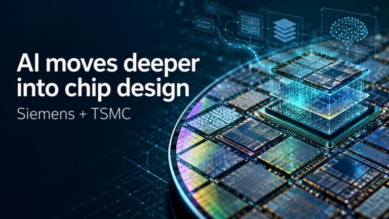
Source: https://semiwiki.com/eda/siemens-eda/374000-siemens-and-tsmc-push-ai-deeper-into-chip-design/
Siemens and TSMC are expanding their collaboration on semiconductor design tools, with a focus on AI assisted workflows, advanced chip packaging and support for newer manufacturing processes. Their announcement centers on an AI agent intended to find and fix design rule violations: errors that can prevent a chip layout from being manufactured as planned.
지멘스(Siemens)와 TSMC가 반도체 설계 툴 분야 협력을 확대하며 AI 지원 워크플로우, 첨단 칩 패키징, 그리고 최신 제조 공정 지원에 주력하고 있습니다. 이번 발표의 핵심은 칩 레이아웃이 계획대로 제조되는 것을 방해할 수 있는 오류인 설계 규칙 위반(Design Rule Violations)을 찾아내고 수정하도록 고안된 AI 에이전트입니다.
The proposed workflow connects Siemens’ Calibre verification software with its Aprisa and Solido design tools. Instead of requiring engineers to diagnose every violation and make each correction by hand, the agent is designed to identify a problem, analyze its context, suggest or carry out a fix, and check the result. Siemens and TSMC say this could reduce manual work and shorten the path to tapeout, when a finished design is sent for manufacturing.
제안된 워크플로우는 지멘스의 칼리버(Calibre) 검증 소프트웨어를 아프리사(Aprisa) 및 솔리도(Solido) 설계 툴과 연결합니다. 엔지니어가 모든 위반 사항을 직접 진단하고 수작업으로 수정하는 대신, 이 에이전트는 문제를 파악하고, 그 맥락을 분석하며, 수정안을 제안하거나 직접 실행한 뒤 결과를 확인하도록 설계되었습니다. 지멘스와 TSMC는 이를 통해 수작업을 줄이고, 완성된 설계를 제조 공장으로 보내는 테이프아웃(Tapeout)까지의 과정을 단축할 수 있다고 밝힙니다.
That is a meaningful target. Modern chips contain enormous numbers of features, and each new manufacturing process comes with detailed rules governing how those features can be placed and connected. A design may work in a simulation yet still fail a manufacturing check. Fixing one violation can also create another or affect power use, speed or chip area. Verification is therefore an iterative part of development, not a box engineers tick at the end.
이는 의미 있는 목표입니다. 현대의 칩에는 엄청난 수의 기능이 담겨 있으며, 새로운 제조 공정마다 이러한 기능들을 배치하고 연결하는 방법에 대한 세부적인 규칙이 따릅니다. 설계는 시뮬레이션상에서 잘 작동하더라도 제조 검증에서는 실패할 수 있습니다. 또한 하나의 위반 사항을 수정하다가 다른 위반이 발생하거나 전력 사용량, 속도, 칩 면적에 영향을 미칠 수도 있습니다. 따라서 검증은 엔지니어들이 막바지에 체크표시만 하고 끝내는 단계가 아니라, 개발 과정에서 반복적으로 이루어지는 핵심 과정입니다.
The companies describe a broader ambition for Siemens’ Fuse EDA AI system: agents that can work through long, multistep tasks across several tools and validate their own outputs. The collaboration also covers custom chip design and the placement and routing of digital circuits. The practical question is how reliably these systems can handle real projects, where an apparently simple correction may have consequences elsewhere in the design. The announcement describes capabilities and expected benefits, but does not provide customer results showing how much time or cost they save.
양사는 지멘스의 퓨즈(Fuse) EDA AI 시스템에 대한 더 넓은 포부를 밝혔습니다. 여러 툴에 걸쳐 길고 다단계로 이뤄진 작업을 수행하고 자신의 출력값을 스스로 검증할 수 있는 에이전트들이 그것입니다. 이번 협력은 커스텀 칩 설계와 디지털 회로의 배치 및 라우팅(Placement and Routing)도 아우르고 있습니다. 현실적인 과제는 이러한 시스템이 실제 프로젝트를 얼마나 안정적으로 처리할 수 있는가에 있습니다. 겉보기에는 단순해 보이는 수정이 설계의 다른 부분에 예기치 않은 파장을 일으킬 수 있기 때문입니다. 이번 발표에서는 기능과 기대되는 이점이 설명되었지만, 시간이나 비용을 얼마나 절감할 수 있는지 보여주는 고객사 실적 결과는 제공되지 않았습니다.
The work extends beyond AI. Siemens says its tools support several TSMC process technologies and aspects of TSMC’s 3DFabric packaging platform. In 3D designs, engineers may stack chips or connect separate pieces of silicon, often called chiplets, within one package. Those choices introduce challenges involving connections between chips, signal quality and heat. Siemens reports expanded verification support for stacked designs, thermal analysis work and continuing development of chip and package design flows. Some capabilities have been certified for particular TSMC technologies; others remain under development or certification.
이번 협력은 AI에만 국한되지 않습니다. 지멘스는 자사 툴이 여러 TSMC 공정 기술과 TSMC의 3D 패브릭(3DFabric) 패키징 플랫폼의 측면들을 지원한다고 밝혔습니다. 3D 설계에서는 엔지니어들이 하나의 패키지 안에서 칩을 적층하거나 칩렛(Chiplets)이라고 불리는 별개의 실리콘 조각들을 연결할 수 있습니다. 이러한 선택은 칩 간 연결, 신호 품질, 열(Heat)과 관련된 과제들을 수반합니다. 지멘스는 적층 설계에 대한 검증 지원 확대, 열 분석 작업, 그리고 칩 및 패키지 설계 플로우의 지속적인 개발 소식을 전했습니다. 일부 기능은 특정 TSMC 기술에 대해 인증을 받았지만, 여전히 개발 중이거나 인증 단계에 있는 기능도 있습니다.
Why it matters
Chip design is becoming a coordination problem as much as a drawing problem. Engineers must balance performance, energy use, manufacturability, reliability and heat, often across multiple pieces of silicon. Advanced packaging can improve what a system can do, but it also creates more interfaces to check and more ways for one design decision to affect another. Better connected design and verification tools could help teams catch problems earlier, when changes are easier to make.
칩 설계는 이제 도면을 그리는 문제인 동시에 '조정(Coordination)'의 문제가 되어가고 있습니다. 엔지니어들은 종종 여러 조각의 실리콘에 걸쳐 성능, 에너지 소비, 제조 용이성, 신뢰성, 발열 문제를 균형 있게 조율해야 합니다. 첨단 패키징은 시스템의 성능을 향상시킬 수 있지만, 동시에 검증해야 할 인터페이스를 늘리고 하나의 설계 결정이 다른 곳에 영향을 미칠 가능성도 높입니다. 서로 긴밀하게 연결된 설계 및 검증 툴은 팀이 문제를 더 일찍, 즉 변경 작업이 훨씬 수월할 때 발견하도록 도울 수 있습니다.
The collaboration also shows where AI may find a useful role in engineering. A design rule violation has a specific context and a result that can be checked with established software. That gives an AI agent a bounded task and a way to test its work. Even so, a passing check does not prove that a change is the best choice for the whole chip. Engineers will still need to judge trade-offs, especially when a fix affects timing, power or reliability.
이번 협력은 또한 AI가 엔지니어링 분야에서 유용한 역할을 찾을 수 있는 지점을 보여줍니다. 설계 규칙 위반은 명확한 맥락과 검증 가능한 결과를 가지고 있습니다. 이는 AI 에이전트에게 제한된 범위의 작업과 그 작업을 테스트할 수 있는 수단을 제공합니다. 그렇다 하더라도 통과 검증이 곧 그 변경이 전체 칩 입장에서 최선의 선택임을 증명하는 것은 아닙니다. 특히 수정이 타이밍, 전력, 신뢰성에 영향을 미칠 때 엔지니어들은 여전히 상충 관계(Trade-off)를 판단해야 할 것입니다.
There is an ecosystem effect, too. When design tools are certified for a manufacturer’s processes and packaging technologies, chip companies can use those flows with greater confidence. Siemens and TSMC are also extending training resources to TSMC design partners, which may help more teams learn the methods needed for advanced nodes.
생태계 측면의 효과도 존재합니다. 설계 툴이 제조사의 공정 및 패키징 기술에 대해 인증을 받으면, 칩 제조 기업들은 더 높은 신뢰를 가지고 해당 플로우를 사용할 수 있습니다. 지멘스와 TSMC는 또한 교육 리소스를 TSMC 설계 파트너들에게까지 확대하고 있으며, 이는 더 많은 팀이 첨단 노드에 필요한 방법론을 익히는 데 도움을 줄 수 있습니다.
Bottom line: For chipmakers, the value of this announcement will ultimately depend on measured results: fewer hours spent resolving violations, faster design cycles, and chips that meet their targets when manufactured. The companies have outlined an ambitious direction. The next test is whether these connected tools deliver those gains consistently on complex customer designs.
결론: 칩 제조사들에게 있어 이번 발표의 가치는 결국 측정 가능한 결과에 달려 있습니다. 위반 사항을 해결하는 데 소요되는 시간 감소, 더 빨라진 설계 주기, 그리고 제조되었을 때 목표 성능을 정확히 충족하는 칩이 그것입니다. 양사는 야심찬 방향성을 제시했습니다. 다음 관문은 이러한 연결된 툴들이 복잡한 고객 설계 상에서 실제로 그러한 이점들을 일관되게 전달할 수 있는지를 증명하는 것입니다.



