Smoothing the Quantum Path: ASML and Xanadu Target Photon Loss
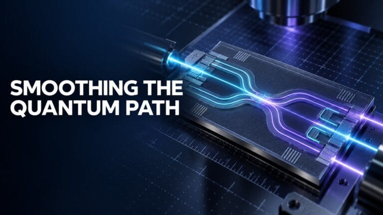
ASML’s decision to collaborate with Xanadu targets one of photonic quantum computing’s most unforgiving engineering constraints: photon loss. The companies will investigate advanced lithography processes for Xanadu’s photonic quantum hardware, focusing on whether tighter patterning control can suppress loss mechanisms and improve the prospects for fault-tolerant, utility-scale machines.
ASML이 자나두(Xanadu)와 협력하기로 한 결정은 광자 기반 양자 컴퓨팅의 가장 가혹한 엔지니어링 제약 중 하나인 '광자 손실(photon loss)'을 겨냥하고 있습니다. 두 회사는 자나두의 광자 양자 하드웨어를 위한 첨단 리소그래피 공정을 연구할 예정이며, 더 엄격한 패턴 제어를 통해 손실 메커니즘을 억제하고 결함 허용(fault-tolerant)이 가능하며 실용적인 규모의 머신을 구현할 가능성을 높이는 데 초점을 맞추고 있습니다.
Photonic quantum processors encode and manipulate quantum information in states of light. Their appeal is substantial: photons move quickly, interact weakly with the environment and can support room-temperature system architectures. Xanadu combines sources, interferometers, switches, detectors and optical interconnects to generate and process entangled states. Yet the same weak interaction that protects photons from environmental noise makes lost photons difficult to recover. Absorption, scattering, imperfect coupling and component inefficiency can remove carriers of quantum information before computation is complete.
광자 양자 프로세서는 빛의 상태로 양자 정보를 인코딩하고 조작합니다. 그 매력은 상당합니다. 광자는 빠르게 이동하고, 환경과의 상호작용이 약하며, 상온 시스템 아키텍처를 지원할 수 있습니다. 자나두는 광원, 간섭계, 스위치, 검출기, 광학 상호 연결을 결합하여 얽힌 상태(entangled states)를 생성하고 처리합니다. 그러나 광자를 환경 노이즈로부터 보호하는 바로 그 약한 상호작용 때문에 잃어버린 광자는 복구하기가 어렵습니다. 흡수, 산란, 불완전한 결합, 그리고 소자의 비효율성은 연산이 완료되기도 전에 양자 정보의 전달체를 소실시킬 수 있습니다.
Loss compounds rapidly as circuits grow. If a photon survives each of N sequential components with probability η, the end-to-end survival probability scales approximately as η^N. Even a small per-component penalty therefore becomes severe in deep circuits. Lost photons reduce successful sampling rates, degrade entanglement and consume error-correction resources. Fault-tolerant architectures can tolerate finite loss, but only below architecture-dependent thresholds and with considerable overhead. Better fabrication attacks the problem at its physical source.
회로가 커질수록 손실은 기하급수적으로 누적됩니다. 광자가 $N$개의 순차적 구성 요소 각각을 확률 η로 통과해 살아남는다면, 전체 생존 확률은 대략 η^N으로 스케일링됩니다. 따라서 구성 요소당 발생하는 작은 손실조차도 심층 회로에서는 심각한 문제가 됩니다. 손실된 광자는 성공적인 샘플링 비율을 떨어뜨리고, 얽힘을 저하시키며, 오류 정정 자원을 소모합니다. 결함 허용 아키텍처는 유한한 손실을 감내할 수 있지만, 이는 아키텍처 의존적 임계값 이하일 때 그리고 상당한 오버헤드를 감수할 때만 가능합니다. 더 나은 제조 공정은 그 물리적 근원에서부터 이 문제를 해결합니다.
The ASML-Xanadu program specifically connects optical loss with line-edge roughness, or LER. Lithography defines the lateral boundaries of waveguides and other nanophotonic structures. Real edges contain nanoscale deviations from the intended geometry because of exposure, resist chemistry, development and pattern-transfer effects. These deviations perturb the waveguide’s refractive-index boundary, coupling guided light into radiation modes or producing back-scattering. The resulting propagation loss is especially consequential when light traverses long routes, resonant structures or many repeated components.
ASML-자나두 프로그램은 특히 광학적 손실을 선폭 거칠기(line-edge roughness, LER)와 연결합니다. 리소그래피는 도파관 및 기타 나노포토닉 구조의 측면 경계를 정의합니다. 실제 모서리는 노광, 레지스터 화학, 현상 및 패턴 전송 효과로 인해 의도된 기하학적 형상에서 나노미터 단위의 편차를 포함합니다. 이러한 편차는 도파관의 굴절률 경계를 교란하여 유도광을 복사 모드로 결합하거나 후방 산란을 발생시킵니다. 그 결과 발생하는 전파 손실은 빛이 긴 경로, 공진 구조 또는 반복되는 많은 구성 요소를 통과할 때 특히 중대한 영향을 미칩니다.
Reducing LER is not simply a matter of printing smaller features. Engineers must optimize the full patterning stack: exposure conditions, mask design, resist selection, stochastic variability, etch bias, sidewall profile and process control. Critical-dimension uniformity also matters because variations shift optical phase, splitting ratios and resonance frequencies. A process can meet nominal linewidth targets yet still deliver poor quantum performance if edge spectra, sidewall angles or wafer-scale uniformity are uncontrolled.
LER을 줄이는 것은 단순히 더 작은 패턴을 인쇄하는 것만이 아닙니다. 엔지니어들은 노광 조건, 마스크 디자인, 레지스트 선택, 확률적 변동성, 식각 편차(etch bias), 측벽 프로파일, 공정 제어에 이르기까지 전체 패터닝 스택을 최적화해야 합니다. 임계 치수 균일성(critical-dimension uniformity) 역시 중요합니다. 변동은 광학적 위상, 분할비, 공진 주파수를 변화시키기 때문입니다. 모서리 스펙트럼, 측벽 각도 또는 웨이퍼 전반의 균일성이 제어되지 않는다면, 공정이 명목상의 선폭 목표를 충족하더라도 저조한 양자 성능을 낼 수 있습니다.
ASML brings expertise in lithographic imaging, process windows, metrology and computational correction. Xanadu contributes device requirements, photonic circuit designs and quantum-level performance data. Together, they can connect manufacturing variables to optical figures of merit rather than treating lithography and quantum architecture as separate optimization problems. Useful experiments could correlate measured LER power spectra with waveguide attenuation, quantify sensitivity to pattern-transfer steps and establish design rules that trade density against loss and yield.
ASML은 리소그래피 이미징, 공정 윈도우, 계측 및 연산 보정 분야의 전문성을 제공합니다. 자나두는 소자 요구사항, 광자 회로 설계, 그리고 양자 수준의 성능 데이터를 기여합니다. 두 회사는 리소그래피와 양자 아키텍처를 별개의 최적화 문제로 다루는 대신, 제조 변수를 광학적 성능 지표와 연결할 수 있습니다. 유효한 실험을 통해 측정된 LER 파워 스펙트럼을 도파관 감쇠와 상관시키고, 패턴 전송 단계에 대한 민감도를 정량화하며, 밀도와 손실 및 수율 간의 트레이드오프를 규정하는 설계 규칙을 수립할 수 있습니다.
The collaboration does not mean ASML is building a quantum computer, nor does the announcement specify a production node, tool platform or numerical loss target. It is a research effort to understand which lithography-enabled approaches can produce lower-loss photonic structures. That distinction matters: ultra-fine resolution alone does not guarantee smooth interfaces, and laboratory improvements must ultimately transfer to stable, high-yield manufacturing.
이번 협력이 ASML이 양자 컴퓨터를 제작한다는 것을 의미하지는 않으며, 발표 내용에 생산 노드, 툴 플랫폼 또는 수치적 손실 목표가 명시되어 있는 것도 아닙니다. 이는 리소그래피 기반 접근 방식을 통해 더 낮은 손실의 광자 구조를 생성할 수 있는 방안을 이해하기 위한 연구 노력입니다. 이러한 구별은 중요합니다. 초미세 해상도만으로는 매끄러운 계면이 보장되지 않으며, 실험실에서의 개선 사항은 결국 안정적이고 수율이 높은 제조 공정으로 이전되어야 합니다.
Commercially relevant photonic quantum systems will require repeatable fabrication across many dies, modules and wafers. Variability that is acceptable in classical photonics may be costly when thousands or millions of optical operations contribute to one error-corrected computation. Process improvements can create system-level leverage by increasing photon survival, reducing calibration burden and lowering the number of physical resources required per logical qubit.
상업적으로 의미 있는 광자 양자 시스템은 다수의 다이, 모듈, 웨이퍼에 걸쳐 반복 가능한 제조 공정을 필요로 합니다. 고전 광학에서는 허용될 수 있는 변동성이 수천 또는 수백만 건의 광학 연산이 하나의 오류 정정 연산에 기여할 때는 막대한 비용을 초래할 수 있습니다. 공정 개선은 광자 생존율을 높이고, 보정 부담을 줄이며, 논리적 큐비트당 요구되는 물리적 자원의 수를 낮추어 시스템 수준의 레버리지 효과를 창출할 수 있습니다.
Success will also depend on packaging, fiber-to-chip coupling, detector efficiency and source quality, which lithography cannot solve alone. Still, lowering on-chip propagation and component loss expands the available system budget, making every downstream engineering compromise easier to manage at scale.
성공 여부는 패키징, 파이버-칩 결합, 검출기 효율, 광원 품질에도 좌우될 것이며, 이는 리소그래피만으로는 해결할 수 없습니다. 그럼에도 불구하고 칩 내 전파 및 소자 손실을 줄이면 사용 가능한 시스템 버짓(system budget)이 넓어져, 다운스트림의 모든 엔지니어링 타협을 대규모 환경에서 더 쉽게 관리할 수 있게 됩니다.
Bottom line: The partnership therefore links semiconductor manufacturing discipline with quantum error-correction economics. If advanced lithography can measurably reduce scattering and device variability, Xanadu may obtain more reliable photonic building blocks, while ASML gains insight into requirements beyond conventional electronic scaling. The immediate outcome is process knowledge, not a finished fault-tolerant machine. But for photonic quantum computing, lowering each fraction of a decibel can translate into a disproportionately larger and more useful processor.
요약하자면: 이번 파트너십은 반도체 제조 규율과 양자 오류 정정 경제학을 연결합니다. 첨단 리소그래피가 산란과 소자 변동성을 측정 가능할 정도로 줄일 수 있다면, 자나두는 더 신뢰할 수 있는 광자 빌딩 블록을 확보할 수 있고, ASML은 전통적인 전자 스케일링을 넘어선 요구사항에 대한 통찰력을 얻게 됩니다. 즉각적인 결과물은 완성이 끝난 결함 허용 기계가 아니라 공정 지식입니다. 그러나 광자 양자 컴퓨팅에게 있어서는, 0.1dB의 작은 분수 단위라도 낮추는 것이 불균형적으로 더 크고 유용한 프로세서로 이어질 수 있습니다.



