Terafab’s Single Roof: Why Packaging, Not Lithography, Decides High Volume
By Shaurya Seth
Terafab is one of the most ambitious projects of the decade: $16.8 billion for phase one and up to $119 billion across four phases. A research fab in Austin iterates on process recipes, transistor designs, and packaging variants at a few thousand wafers per month. A volume fab in Grimes County targets 100,000 wafer starts per month with first silicon targeted for 2029. Elon Musk has named Intel’s 14A as the volume process.
테라팹(Terafab)은 이번 세기 가장 야심 찬 프로젝트 중 하나로, 1단계에만 168억 달러, 4단계에 걸쳐 최대 1190억 달러가 투입됩니다. 오스틴에 위치한 연구용 팹은 월 수천 장의 웨이퍼 규모로 공정 레시피, 트랜지스터 설계, 패키징 변형을 반복적으로 테스트하며 고도화합니다. 그라임스 카운티(Grimes County)에 세워질 양산 팹은 월 10만 장의 웨이퍼 투입(WSPM)을 목표로 하고 있으며, 최초의 실리콘 칩 생산은 2029년으로 예정되어 있습니다. 일론 머스크는 인텔의 14A 공정을 양산 공정으로 지목한 바 있습니다.
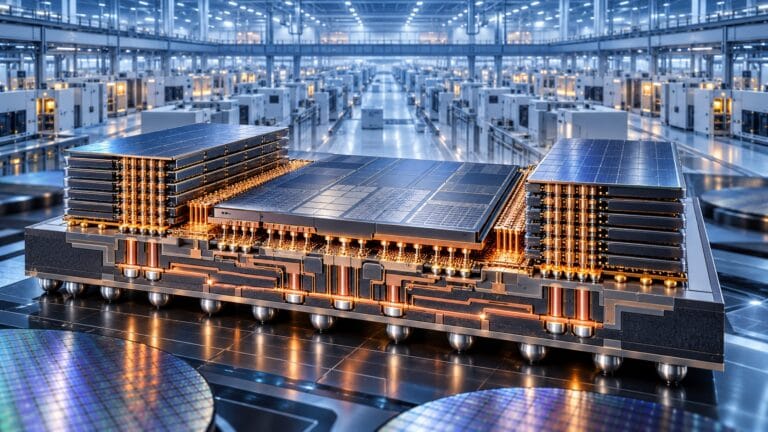
The headline claim is that logic, memory, and advanced packaging will sit under one roof. The advantage: it shortens the loop from mask revision to a packaged part, cuts Q-times between process steps, and lets one engineering organization co-design logic, memory, and package instead of separate companies negotiating process windows across time zones.
이 프로젝트의 핵심 주장인 타이틀은 로직, 메모리, 그리고 첨단 패키징이 한 지붕 아래에 모인다는 것입니다. 그 장점은 마스크 리비전부터 패키징된 부품이 완성될 때까지의 주기를 단축하고, 공정 단계 사이의 대기 시간(Q-time)을 줄이며, 서로 다른 기업들이 시차를 두고 공정 윈도우를 협상하는 대신 하나의 엔지니어링 조직이 로직, 메모리, 패키지를 공동 설계할 수 있게 한다는 점입니다.
But Terafab must build from scratch an ecosystem that already exists worldwide. One roof fixes logistics but does not fix the physics inside the package. Two packaging requirements will decide whether it pays off.
그러나 테라팹은 전 세계에 이미 존재하는 생태계를 처음부터 다시 구축해야 합니다. 한 지붕 아래에 모인다고 해서 물류는 해결되지만 패키지 내부의 물리적 법칙까지 해결되지는 않습니다. 다음 두 가지 패키징 요구 사항이 이 프로젝트의 성패를 가를 것입니다.
Connecting HBM to Logic
HBM stacks are currently joined by Cu pillars with SnAg solder caps, using mass reflow with molded underfill (MR-MUF) or thermal compression with non-conductive film (TC-NCF). As pitch approaches 20 µm, the cap shrinks, and solder bridging becomes the main risk. The path forward is thinner caps, Sn pillars, and eventually solderless Cu-Cu hybrid bonding. My own UCLA work developed Sn pillars to replace solder bumps, targeting 10 µm pitch; 60 µm was the finest that bonded reliably die-to-wafer.
현재 HBM 스택은 몰디드 언더필(MR-MUF) 방식을 사용한 매스 리플로우(mass reflow)나 비전도성 필름(TC-NCF)을 사용한 열압착(thermal compression) 방식을 통해 SnAg 솔더 캡이 달린 Cu 필러로 접합됩니다. 피치(pitch)가 20 µm에 가까워짐에 따라 캡은 작아지고, 솔더 브리징(solder bridging)이 주된 위험 요소가 됩니다. 앞으로 나아갈 방향은 더 얇은 캡, Sn 필러, 그리고 궁극적으로는 솔더가 없는 Cu-Cu 하이브리드 본딩입니다. 저자 자신의 UCLA 연구에서는 솔더 범프를 대체하기 위해 Sn 필러를 개발했으며 10 µm 피치를 목표로 삼았으나, 다이투웨이퍼(die-to-wafer) 방식으로 안정적으로 접합할 수 있었던 가장 미세한 간격은 60 µm였습니다.
Plating sets the limits. Plating taller pillars faster means higher current density, which risks voids, rough tops, and poor within-die height uniformity; co-planarity must stay under 5%.
도금(plating) 공정이 한계를 설정합니다. 더 높은 필러를 더 빠르게 도금한다는 것은 더 높은 전류 밀도를 의미하며, 이는 보이드(void), 거친 표면, 다이 내 높이 균일성 저하의 위험을 초래합니다. 평탄도(co-planarity)는 5% 미만으로 유지되어야 합니다.
JEDEC’s move from a 720 to a 775 µm stack height keeps 16-high HBM4 on micro-bumps and pushes hybrid bonding to later generations, though its density, roughly 14,000 signals/mm² versus about 1,500 for TSV stacking, makes it inevitable. When it arrives, CMP becomes the largest yield variable: dielectric too high and copper never connects; copper too high and voids form. Activated surfaces also degrade while wafers wait, so Q-time becomes a yield parameter.
JEDEC이 스택 높이를 720 µm에서 775 µm로 변경함에 따라 16단 HBM4는 당분간 마이크로 범프를 유지하고 하이브리드 본딩은 차세대 기술로 미뤄지게 되었지만, TSV 적층의 약 1,500 신호/mm²에 비해 약 14,000 신호/mm²에 달하는 고밀도 특성 덕분에 하이브리드 본딩 도입은 불가피합니다. 하이브리드 본딩이 도입되는 시점에는 화학적 기계적 연마(CMP)가 가장 큰 수율 변수가 됩니다. 유전체 높이가 너무 높으면 구리가 결코 연결되지 않고, 구리 높이가 너무 높으면 보이드가 형성됩니다. 또한 웨이퍼가 대기하는 동안 활성화된 표면이 열화되므로 Q-time이 수율 파라미터가 됩니다.
This is where the single roof helps. I would build Terafab’s first product as its own logic plus purchased HBM on a proven 2.5D flow, while the research fab develops hybrid bonding as one co-located CMP, activation, and bonding module with enforced Q-time limits. The catch: tool-to-tool variation. A process proven in Austin must be re-qualified to the same yield in Grimes County.
이 지점이 바로 '한 지붕 아래'라는 조건이 도움이 되는 부분입니다. 저자라면 검증된 2.5D 플로우 상에서 자체 로직과 구매한 HBM을 결합하여 테라팹의 첫 번째 제품을 구축하는 한편, 연구용 팹에서는 엄격한 Q-time 제한을 적용한 동일 위치(co-located) CMP, 표면 활성화 및 본딩 모듈로서 하이브리드 본딩을 개발할 것입니다. 다만 툴과 툴 사이의 편차(tool-to-tool variation)가 함정입니다. 오스틴에서 검증된 공정은 그라임스 카운티에서도 동일한 수율이 나오도록 재인증을 거쳐야 합니다.
Interconnect Reliability
Once bonding works, reliability is next: these chips will run in robots and in orbit.
일단 본딩이 성공하면 다음 과제는 신뢰성입니다. 이 칩들은 로봇과 우주 공간에서 작동할 것입니다.
In 2.5D, the Sn-based joint is the weak point. As pitch shrinks, more of each joint becomes intermetallic after reflow or TCB. Cu₆Sn₅ and Cu₃Sn are brittle; as they grow and coarsen, shear strength falls with each thermal cycle until joints open. Heat accelerates that growth, and Musk says the space chips will run hotter than standard silicon. Higher current density in small bumps adds electromigration voiding. In my Sn-pillar work, die-to-wafer bonds at 60 µm pitch reached 28.26 N in shear testing. But the interfacial IMC, not time-zero strength, sets long-term behavior.
2.5D 패키징에서 Sn 기반 접합부는 취약점입니다. 피치가 줄어들수록 리플로우나 TCB 이후 각 접합부에서 금속간 화합물(IMC)이 차지하는 비중이 커집니다. Cu₆Sn₅와 Cu₃Sn은 취성(brittleness)이 있습니다. 이들이 성장하고 조대화(coarsening)됨에 따라 열 사이클이 반복될수록 전단 강도가 떨어져 결국 접합부가 개방됩니다. 열은 이러한 성장을 가속화하며, 머스크는 우주용 칩이 표준 실리콘보다 더 뜨겁게 동작할 것이라고 밝혔습니다. 작은 범프에서의 높은 전류 밀도는 일렉트로마이그레이션(electromigration)에 의한 보이드 발생을 가중시킵니다. 저자의 Sn 필러 연구에서 60 µm 피치의 다이투웨이퍼 접합은 전단 테스트에서 28.26 N에 도달했습니다. 그러나 초기 강도가 아니라 계면의 금속간 화합물(IMC)이 장기적인 거동을 결정합니다.
Hybrid bonding still poses risks: Cu-Cu interfaces can trap voids, and copper expands against the dielectric during anneal. My approach would be to qualify data center, Optimus, and space parts separately for thermal cycling, electromigration, and high-temperature storage; to treat Ni barriers as a trade-off between slower intermetallic growth and co-planarity; and to plan the move to nanotwinned Cu, which bonds at about 200°C instead of over 300°C.
하이브리드 본딩 역시 위험을 내포하고 있습니다. Cu-Cu 인터페이스는 보이드를 가둘 수 있으며, 구리는 어닐링 과정에서 유전체 방향으로 팽창합니다. 저자의 접근 방식이라면 데이터센터용, 옵티머스(Optimus)용, 우주용 부품의 열 사이클링, 일렉트로마이그레이션, 고온 보관에 대한 인증을 각각 따로 진행하고; Ni 배리어는 금속간 화합물 성장 지연과 평탄도 사이의 트레이드오프로 취급하며; 300°C 이상이 아니라 약 200°C에서 본딩이 가능한 나노쌍정 구리(nanotwinned Cu)로의 전환을 계획할 것입니다.
What Would Work
Terafab’s aim is more than a terawatt of AI compute a year for Optimus, Cybercab, xAI and orbital data centers. Packaging is where that chain is least proven, so I would phase it:
- Buy proven packaging capacity first: Intel EMIB
- Bring 2.5D in-house once research-fab yields match the partner’s.
- Introduce hybrid bonding and nano-twinned Cu only when the co-located bonding module holds yield at volume.
테라팹의 목표는 옵티머스, 사이버캡(Cybercab), xAI, 그리고 우주 데이터센터를 위해 연간 1테라와트 이상의 AI 연산 능력을 공급하는 것입니다. 패키징은 이 공급망에서 가장 검증되지 않은 부분이므로, 저자라면 다음과 같이 단계별로 접근할 것입니다.
- 먼저 검증된 패키징 역량을 구매합니다: 인텔 EMIB 활용
- 연구용 팹의 수율이 협력사의 수준과 일치하게 되면 2.5D 패키징을 사내로 들여옵니다.
- 동일 위치의 본딩 모듈이 양산 수율을 안정적으로 유지할 때만 하이브리드 본딩과 나노쌍정 구리를 도입합니다.
Today, the site and phase-one funding are approved, and the research fab is under construction, but no first-wafer date or ownership terms are public, and neither Tesla nor Intel is contractually bound. One roof shortens the learning cycle; packaging decides whether it pays off.
현재 부지와 1단계 자금은 승인되었고 연구용 팹은 건설 중이지만, 최초 웨이퍼 생산일이나 소유권 조건은 공개된 바 없으며 테슬라와 인텔 모두 계약상 구속되어 있지 않습니다. 한 지붕 아래에 모이는 것은 학습 주기를 단축시켜 주지만, 그 성공 여부를 결정하는 것은 결국 패키징입니다.
Shaurya Seth is a Senior Process Integration Engineer at Analog Devices, where he develops BEOL processes for mature-node devices used in power electronics applications. He holds an M.S. in Materials Science and Engineering from UCLA, where his CHIPS lab thesis developed Sn electroplating for fine-pitch advanced packaging interconnects. He has published peer-reviewed research and conducted reviews for IEEE Transactions on Semiconductor Manufacturing, Journal of Applied Physics, and Materials Today Electronics.
샤우랴 세트(Shaurya Seth)는 아날로그 디바이스(Analog Devices)의 선임 공정 통합 엔지니어로서 전력 전자 응용 분야에 사용되는 성숙 노드(mature-node) 소자를 위한 BEOL 공정을 개발하고 있습니다. 그는 UCLA에서 재료과학공학 석사 학위를 취득했으며, 당시 CHIPS 연구실의 학위 논문에서 미세 피치 첨단 패키징 인터커넥트를 위한 Sn 전기도금을 개발했습니다. 동료 평가를 거친 연구 논문을 다수 발표했으며, IEEE Transactions on Semiconductor Manufacturing, Journal of Applied Physics, Materials Today Electronics 등의 저널에서 심사위원으로 활동했습니다.
The views, thoughts, and opinions expressed belong solely to the speaker, and not to the speaker’s employer, organization, committee or any other group or individual.
본문에 표현된 견해, 생각, 의견은 전적으로 발표자 개인의 것이며, 발표자의 고용주, 소속 조직, 위원회 또는 기타 단체나 개인의 공식 입장을 대변하지 않습니다.



