The $725 Million Chip Development: Why Execution Risk, Not IP Cost, Now Dictates Advanced-Node Survival
The philosophy of relying on a single, unified IP stack to lower your total cost of ownership is not a new concept invented just for the AI era. Semiconductor engineering teams have been weighing the trade-offs of piecemeal versus integrated intellectual property sourcing for decades. In previous process generations, veering away from a unified platform to cherry-pick individual components was often a tolerable compromise. The resulting vendor integration friction was an annoying operational tax, but it was rarely a fatal one.
단일 통합 IP 스택에 의존하여 총소유비용(TCO)을 낮추는 철학은 AI 시대를 위해 특별히 발명된 새로운 개념이 아닙니다. 반도체 엔지니어링 팀들은 수십 년 동안 개별(piecemeal) IP 소싱과 통합 IP 소싱 사이의 장단점을 저울질해 왔습니다. 이전 공정 세대에서는 단일화된 플랫폼에서 벗어나 개별 부품을 입맛대로 골라 쓰는(cherry-pick) 방식이 대개 용인할 만한 타협점이었습니다. 그 결과로 발생하는 벤더 간 통합 마찰은 성가신 운영상의 세금 같았지만, 치명적인 경우는 드물었습니다.
In the AI era, however, that calculus has fundamentally shifted. As design costs surge toward three-quarters of a billion dollars at the 2nm node, and complex AI workloads push power delivery, operating voltage, and process variation to their absolute physical limits, the financial penalty for execution friction has been dramatically amplified. What was once a manageable integration headache has now become a multi-hundred-million-dollar program killer.
그러나 AI 시대에 이르러 이러한 계산법은 근본적으로 바뀌었습니다. 2nm 노드에서 설계 비용이 7억 5천만 달러에 육박하고, 복잡한 AI 워크로드가 전력 공급, 동작 전압, 공정 편차를 절대적인 물리적 한계까지 밀어붙이면서 실행 마찰에 대한 재정적 페널티가 극적으로 증폭되었습니다. 한때 감당할 수 있었던 통합의 골칫거리가 이제는 수억 달러 규모의 프로젝트를 좌초시키는 주범이 되었습니다.
The Silent Economics of Advanced Process Nodes
Historically, engineering teams spent their development cycles comparing individual IP licensing fees line by line. However, as the semiconductor industry accelerates through sub-5nm territories into 3nm and 2nm nodes, that traditional accounting model breaks down completely. Research from International Business Strategies highlights a steep cost trajectory. Where designing a large 28nm SoC from scratch cost roughly $48 million, that figure jumped to $249 million at 7nm, $449 million at 5nm, $581 million at 3nm, and is now projected to reach an astronomical $725 million at 2nm.
역사적으로 엔지니어링 팀은 개발 주기의 라이선스 비용을 항목별로 비교하는 데 시간을 보냈습니다. 그러나 반도체 산업이 5nm 미만을 거쳐 3nm 및 2nm 노드로 가속화됨에 따라 이러한 전통적인 회계 모델은 완전히 무너집니다. International Business Strategies(IBS)의 연구에 따르면 가파른 비용 상승 추세가 두드러집니다. 대형 28nm SoC를 처음부터 설계하는 데 약 4,800만 달러가 들었던 반면, 그 수치는 7nm에서 2억 4,900만 달러, 5nm에서 4억 4,900만 달러, 3nm에서 5억 8,100万 달러로 뛰어올랐으며, 이제 2nm에서는 무려 7억 2,500만 달러에 이를 것으로 예상됩니다.
At these advanced nodes, the line-item license fee of an individual IP block is entirely dwarfed by the massive financial exposure of late-stage execution failures. Sourcing Foundation IP by assembling logic libraries from one vendor, embedded memories from a second, I/Os from a third, and non-volatile memory from a fourth introduces unverified boundary lines across the silicon layout. Every additional vendor interface represents an active seam where schedule delays and integration mismatches accumulate. Engineering teams operating in this fragmented environment frequently contend with mismatched deliverables and documentation, clashing characterization standards, and multiple support queues between suppliers. Furthermore, when integration hurdles emerge or silicon bring-up encounters unexpected behavior, no single vendor owns the root-cause analysis, resulting in fragmented accountability and overwhelming administrative overhead. When high-performance computing and Edge AI workloads push transistors to their physical limits, these late-stage surprises become exponentially more expensive.
이러한 첨단 노드에서는 개별 IP 블록의 항목별 라이선스 비용이 후반부 실행 실패로 인한 막대한 재정적 위험에 완전히 압도당합니다. 한 벤더의 로직 라이브러리, 두 번째 벤더의 임베디드 메모리, 세 번째 벤더의 I/O, 네 번째 벤더의 비휘발성 메모리를 조합하여 파운데이션 IP(Foundation IP)를 소싱하면 실리콘 레이아웃 전반에 걸쳐 검증되지 않은 경계선이 생깁니다. 추가되는 모든 벤더 인터페이스는 일정 지연과 통합 불일치가 누적되는 활성 접점(seam)을 나타냅니다. 이러한 단편화된 환경에서 일하는 엔지니어링 팀은 일치하지 않는 산출물과 문서, 충돌하는 특성화 표준, 공급업체 간의 여러 지원 대기열로 인해 빈번히 어려움을 겪습니다. 더욱이 통합 난관이 발생하거나 실리콘 시동(bring-up)에서 예상치 못한 동작이 발견될 때, 근본 원인 분석을 전담하는 단일 벤더가 없기 때문에 책임 소재가 분산되고 압도적인 행정 오버헤드가 발생합니다. 고성능 컴퓨팅 및 엣지 AI 워크로드가 트랜지스터를 물리적 한계까지 밀어붙일 때, 이러한 후반부의 놀라운 일들은 기하급수적으로 더 비싸집니다.
Quantifying the Execution Exposure
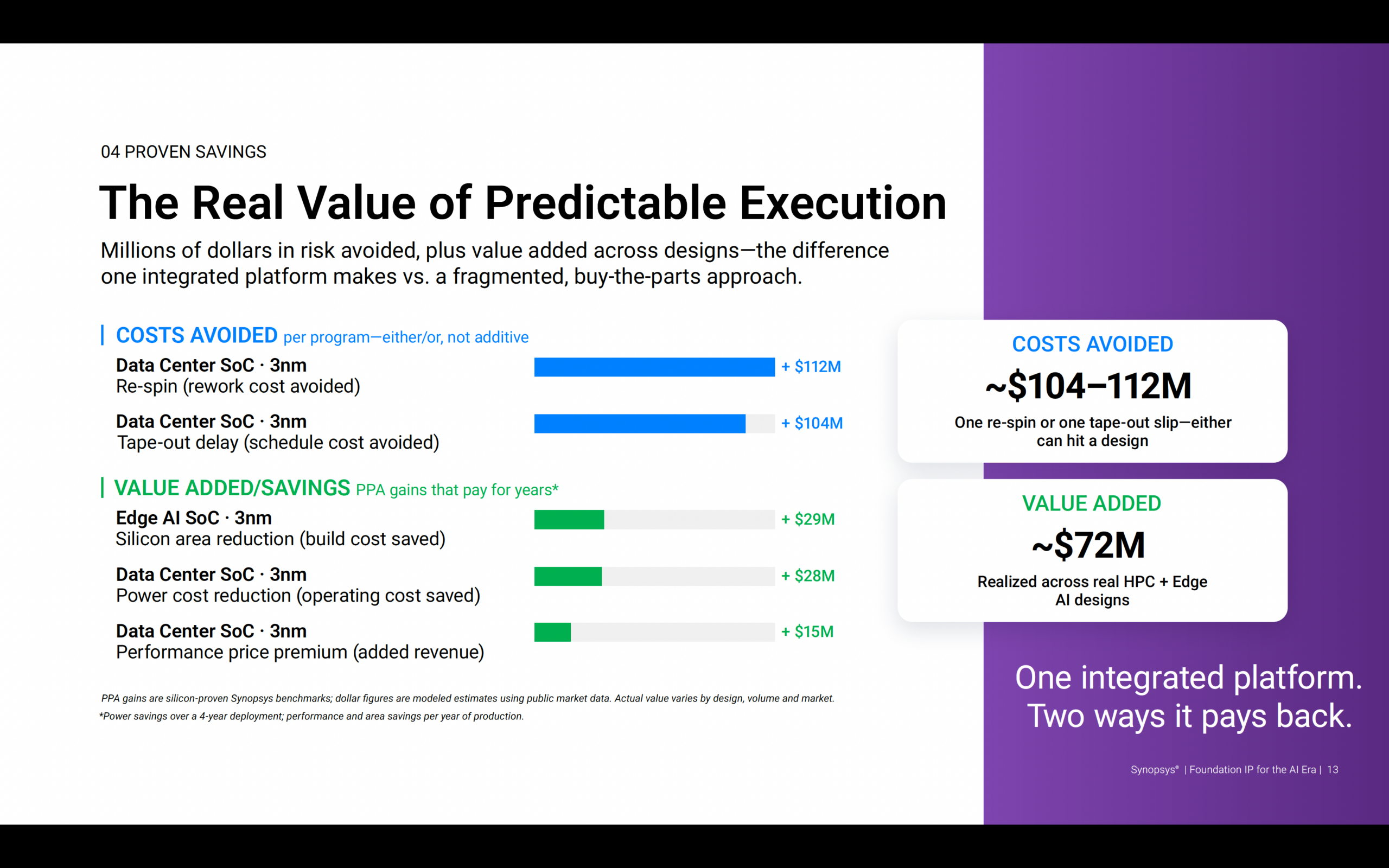
To understand why execution now dictates true total cost of ownership, consider the modeled financial impact of late-stage execution errors on a 3nm Data Center SoC. For a server processor targeting a four-hundred-million-dollar, three-year revenue window, a twenty percent lifecycle delay of approximately 7.2 months puts roughly $80 million in launch revenue at direct risk. When combined with maintaining an engineering team of two hundred developers during the slip, which adds twenty-four million dollars in pure burn rate, the total financial impact reaches one hundred and four million dollars. Missing an initial deployment window often forces a design into a lower-margin quarter or forfeits lead-customer commitments altogether.
실행력이 진정한 총소유비용을 좌우하는 이유를 이해하기 위해, 3nm 데이터 센터 SoC에서 후반부 실행 오류가 미치는 모델링된 재정적 영향을 고려해 보겠습니다. 4억 달러 규모의 3년 매출 창출 기간을 목표로 하는 서버 프로세서의 경우, 약 7.2개월에 달하는 20%의 라이프사이클 지연은 약 8,000만 달러의 출시 매출을 직접적인 위험에 빠뜨립니다. 지연 기간 동안 200명의 개발자로 구성된 엔지니어링 팀을 유지하는 비용(순수 소모 비용 2,400만 달러 추가)과 결합되면, 총 재정적 영향은 1억 400만 달러에 달합니다. 최초 배포 시기를 놓치면 설계를 저마진 분기로 밀어 넣거나 리드 고객 계약을 아예 포기하게 되는 경우가 많습니다.
The ultimate nightmare scenario remains the cost of a silicon re-spin. If bugs or defectivity require an unexpected re-spin, the direct engineering expense of a fifty percent mask set re-work adds roughly $7.5 million in NRE. However, because a re-spin inherently forces that same 7.2-month schedule slip, the combined exposure swells to approximately $112 million. At advanced nodes, a single unbudgeted re-spin can completely wipe out a product line’s profitability or cause executive leadership to cancel the entire program.
최악의 시나리오는 여전히 실리콘 리스핀(re-spin) 비용입니다. 버그나 결함으로 인해 예상치 못한 리스핀이 필요한 경우, 50% 마스크 세트 재작업의 직접적인 엔지니어링 비용은 NRE(비회수성 개발 비용)로 약 750만 달러를 추가합니다. 그러나 리스핀은 본질적으로 동일한 7.2개월의 일정 지연을 강제하므로, 복합적인 위험 노출액은 약 1억 1,200만 달러로 불어납니다. 첨단 노드에서는 예산에 없던 단 한 번의 리스핀만으로도 제품군의 수익성이 완전히 지워지거나 경영진이 전체 프로그램을 취소하게 될 수 있습니다.
The Single-Platform Advantage and Concrete PPA Returns
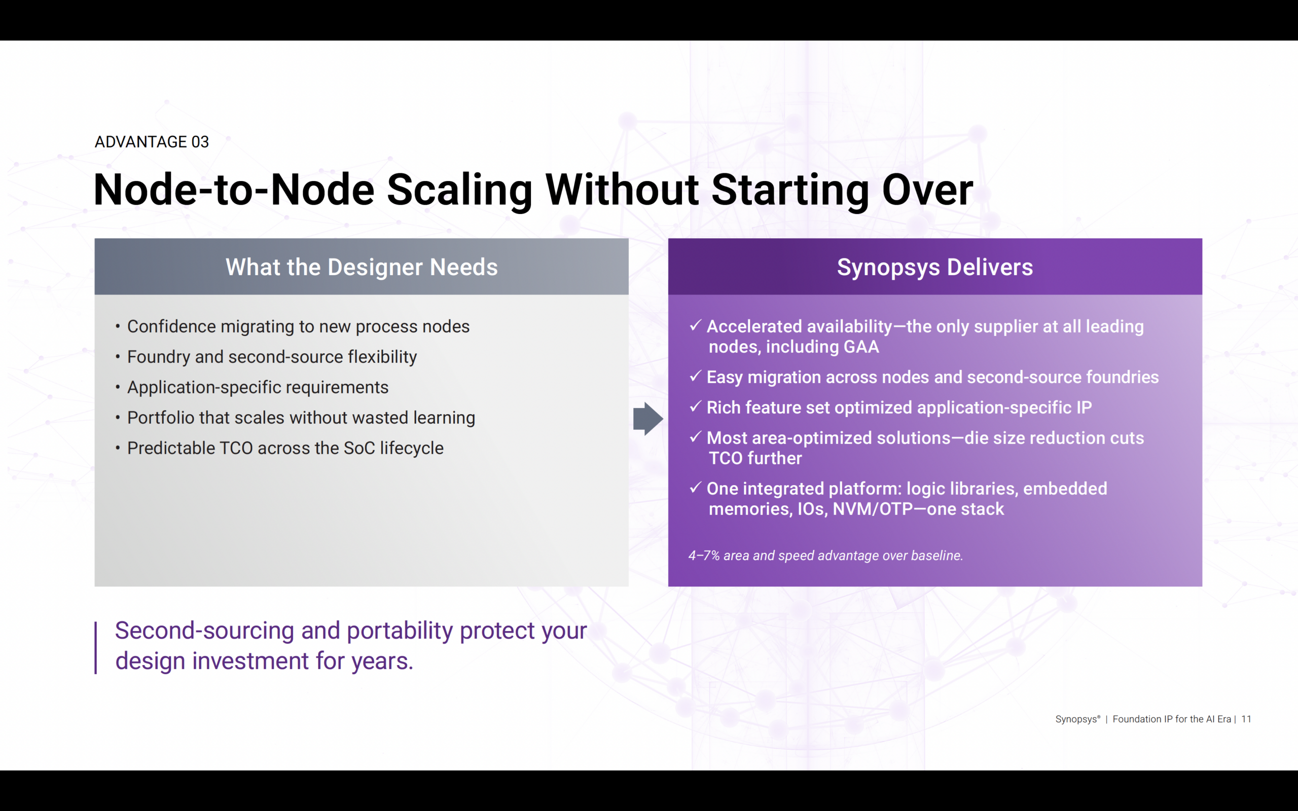
Transitioning from a fragmented basket of parts to a single, integrated Foundation IP platform shifts integration risk back to the IP provider. EDA co-optimized, pre-verified stacks containing logic libraries, embedded memories, I/Os, and NVM OTP eliminate cross-vendor integration seams before they ever reach the design floor. Beyond risk mitigation, co-optimized Foundation IP delivers measurable power, performance, and area returns that compound over production runs. On a 3nm Data Center SoC, a twenty-eight percent reduction in logic library power translates across a hundred-thousand-server deployment into twenty-eight million dollars in saved electricity costs over a four-year lifecycle. Additionally, achieving a six percent performance uplift, assuming a modest three percent price premium, yields fifteen million dollars in added annual revenue across a volume of two-hundred and fifty thousand units per year.
단편화된 부품 바구니에서 단일 통합 파운데이션 IP 플랫폼으로 전환하면 통합 리스크가 다시 IP 공급자에게로 이전됩니다. 로직 라이브러리, 임베디드 메모리, I/O, NVM OTP가 포함된 EDA 공동 최적화(co-optimized), 사전 검증된 스택은 설계 플로에 도달하기도 전에 교차 벤더 간 통합 접점을 제거합니다. 리스크 완화를 넘어, 공동 최적화된 파운데이션 IP는 생산 전반에 걸쳐 복리로 작용하는 측정 가능한 전력, 성능, 면적(PPA) 이점을 제공합니다. 3nm 데이터 센터 SoC에서 로직 라이브러리 전력의 28% 절감은 10만 대의 서버 배포 전반에 걸쳐 4년 라이프사이클 동안 2,800만 달러의 전기 요금 절감으로 이어집니다. 또한, 6%의 성능 향상을 달성하고 소폭의 3% 가격 프리미엄을 가정하면, 연간 25만 대의 볼륨에서 연간 1,500만 달러의 추가 매출이 창출됩니다.
These efficiency gains extend directly into edge applications as well. On a 3nm Edge AI SoC shipping twenty million units annually, an eleven percent reduction in memory area shrinks the overall die size, saving twenty-nine million dollars per year in silicon wafer costs. Synopsys Foundation IP delivers a four to seven percent area and speed advantage over baseline and supports every leading node, including Gate-All-Around architectures. PPA gains are silicon-proven Synopsys benchmarks; dollar figures are modeled estimates based on public market data and will vary by design, volume, and market.
이러한 효율성 향상은 엣지 애플리케이션으로도 직접 이어집니다. 연간 2,000만 대를 출하하는 3nm 엣지 AI SoC에서 메모리 면적의 11% 감소는 전체 다이(die) 크기를 줄여 실리콘 웨이퍼 비용을 연간 2,900만 달러 절감합니다. 시놉시스(Synopsys) 파운데이션 IP는 베이스라인 대비 4~7%의 면적 및 속도 이점을 제공하며, 게이트 올 어라운드(GAA) 아키텍처를 포함한 모든 주요 노드를 지원합니다. PPA 향상 효과는 실리콘으로 검증된 시놉시스 벤치마크이며, 달러 수치는 공개 시장 데이터를 기반으로 한 모델링 추정치로서 설계, 볼륨, 시장에 따라 달라질 수 있습니다.
For a comprehensive look at how a unified IP strategy extends beyond Foundation IP to encompass high-speed interface IP, security subsystems, multi-die chiplets, and Silicon Lifecycle Management (SLM), read the SemiWiki post: [The Architecture of Success: Why a Unified Semiconductor IP Strategy Is the Foundation of Modern SoC Design].
단일 IP 전략이 파운데이션 IP를 넘어 고속 인터페이스 IP, 보안 서브시스템, 멀티 다이 칩렛, 실리콘 라이프사이클 관리(SLM)를 아우르는 방법에 대한 종합적인 내용은 SemiWiki 게시글 **[The Architecture of Success: Why a Unified Semiconductor IP Strategy Is the Foundation of Modern SoC Design]**을 참조하십시오.
Rethinking IP Strategy for First-Pass Success
Sourcing core logic libraries, embedded memories, I/Os, and non-volatile memory is no longer a downstream procurement line item. It is the bedrock of the entire system strategy. Because Foundation IP sets the physical, thermal, power, and voltage boundaries for the entire System-on-Chip, decisions made at this layer dictate what is architecturally possible across the rest of the design. A power reduction in logic libraries or near-threshold voltage tuning does not merely save battery life; it unlocks the power and thermal budget required to deploy high-throughput interface IP like PCIe, CXL, and UCIe chiplets, as well as advanced security subsystems, without hitting a physical thermal wall. Conversely, a mismatch in basic cell characterization or memory timing ripples upward, compromising high-speed interfaces and full-system reliability.
코어 로직 라이브러리, 임베디드 메모리, I/O, 비휘발성 메모리를 소싱하는 것은 더 이상 다운스트림 조달 항목이 아닙니다. 그것은 전체 시스템 전략의 기반입니다. 파운데이션 IP가 전체 시스템온칩(SoC)의 물리적, 열적, 전력, 전압 경계를 설정하기 때문에 이 계층에서 이루어진 결정은 설계의 나머지 부분에서 아키텍처적으로 무엇이 가능한지를 좌우합니다. 로직 라이브러리의 전력 절감이나 문턱 전압 근처(near-threshold) 튜닝은 단순히 배터리 수명을 절약하는 데 그치지 않고, 물리적인 열적 한계에 부딪히지 않으면서 PCIe, CXL, UCIe 칩렛과 같은 고속 인터페이스 IP 및 고급 보안 서브시스템을 배치하는 데 필요한 전력 및 발열 예산을 확보해 줍니다. 반대로, 기본 셀 특성화나 메모리 타이밍의 불일치는 위쪽으로 파급되어 고속 인터페이스와 전체 시스템 신뢰성을 손상시킵니다.
Summary
As design costs approach three-quarters of a billion dollars for a large 2nm SoC, semiconductor business models can no longer absorb integration friction. In the AI era, chip profitability is won or lost in execution, not in individual IP licensing fees. Because Foundation IP is the foundation of everything, getting this baseline layer right is the single most critical decision an engineering leadership team can make. Securing sign-off-ready characterization, enforcing a zero silicon-defect methodology, and establishing single-vendor accountability remains the most predictable path to protecting product margins and ensuring full-system success.
대형 2nm SoC의 설계 비용이 7억 5천만 달러에 육박함에 따라, 반도체 비즈니스 모델은 더 이상 통합 마찰을 감당할 수 없습니다. AI 시대에 칩의 수익성은 개별 IP 라이브러리 비용이 아니라 실행력에서 승패가 갈립니다. 파운데이션 IP가 모든 것의 토대이기 때문에, 이 기준선 계층을 제대로 구축하는 것은 엔지니어링 리더십 팀이 내릴 수 있는 가장 중요한 결정입니다. 사인오프(sign-off) 준비가 완료된 특성화를 확보하고, 제로 실리콘 결함 방법론을 시행하며, 단일 벤더 책임 체제를 구축하는 것은 제품 마진을 보호하고 전체 시스템 성공을 보장하는 가장 예측 가능한 경로입니다.
Download the Synopsys eBook “Foundation IP for the AI Era”
Learn more about Synopsys Foundation IP portfolio.



