The Pivotal Moments That Gave Rise to Silicon Valley

The little-known decisions and breakthroughs—and the remarkable role of Robert Noyce—that helped shape the modern semiconductor industry
by Sunil Mehta
현대 반도체 산업을 형성하는 데 기여한 잘 알려지지 않은 결정과 돌파구—그리고 로버트 노이스(Robert Noyce)의 놀라운 역할
저자: 수닐 메타(Sunil Mehta)
When people tell the story of how Silicon Valley came into being, they usually begin with a familiar sequence of events.
실리콘밸리가 어떻게 탄생하게 되었는지에 대한 이야기를 할 때, 사람들은 대개 익숙한 일련의 사건들로 시작하곤 합니다.
The transistor was invented at Bell Labs. William Shockley moved to California and founded Shockley Semiconductor. Eight of his brilliant young employees rebelled and left to form Fairchild Semiconductor. Fairchild pioneered silicon transistors and the integrated circuit. Gordon Moore formulated what became known as Moore’s Law, charting an exponential trajectory of transistor growth that would guide the semiconductor industry for more than six decades. Robert Noyce and Moore left Fairchild and founded Intel. And Intel went on to launch the microprocessor revolution.
트랜지스터가 벨 연구소(Bell Labs)에서 발명되었습니다. 윌리엄 쇼클리(William Shockley)가 캘리포니아로 이주하여 쇼클리 반도체를 설립했습니다. 그의 명민한 젊은 직원 8명이 반기를 들고 회사를 나와 페어차일드 반도체(Fairchild Semiconductor)를 설립했습니다. 페어차일드는 실리콘 트랜지스터와 집적회로(IC)의 선구자 역할을 했습니다. 고든 무어(Gordon Moore)는 60년 이상 반도체 산업을 이끌게 될 트랜지스터 성장의 지수 함수적 궤적을 제시한, 이른바 '무어의 법칙'을 정립했습니다. 로버트 노이스와 무어는 페어차일드를 떠나 인텔(Intel)을 설립했습니다. 그리고 인텔은 마이크로프로세서 혁명을 주도했습니다.
It is a good high-level account. But history viewed from 30,000 feet can make events look almost inevitable. This is not quite the way it transpired.
이는 꽤 그럴듯한 거시적 설명입니다. 하지만 3만 피트 상공에서 내려다보는 듯한 거시적 역사관은 사건들을 거의 필연적인 것처럼 보이게 만듭니다. 그러나 실제 역사는 그렇게 흘러가지 않았습니다.
While researching my novel, The Compass, which explores key episodes in the lives of Albert Einstein, Robert Noyce and Steve Jobs, I was fascinated to discover what lay beneath this familiar Silicon Valley narrative. What I found was a succession of chance encounters, risky decisions and technological breakthroughs—moments when events could easily have taken another course.
알베르트 아인슈타인, 로버트 노이스, 스티브 잡스의 삶 속 핵심적인 에피소드를 다루는 소설 《더 컴퍼스(The Compass)》를 집필하기 위해 조사하던 중, 저는 이 익숙한 실리콘밸리 내러티브의 이면에 숨겨진 사실들을 발견하고 매료되었습니다. 제가 발견한 것은 우연한 만남, 위험한 결단, 그리고 기술적 돌파구들의 연속이었습니다. 즉, 사건들이 얼마든지 다른 방향으로 흘러갈 수 있었던 순간들이었습니다.
And one man was at the center of an extraordinary number of those pivotal moments: Robert Noyce.
그리고 그 수많은 결정적 순간들의 중심에는 한 인물이 있었습니다. 바로 로버트 노이스였습니다.
The Transistor Comes to Iowa
The story begins far from California.
이야기는 캘리포니아에서 아주 먼 곳에서 시작됩니다.
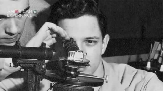
As an undergraduate at Grinnell College in Iowa, Noyce studied physics under Professor Grant Gale. Gale had previously studied with John Bardeen, who in 1947 had helped invent the transistor at Bell Labs with Walter Brattain. After learning of the invention, Gale wrote to Bell Labs asking for a couple of the new devices. There were none to spare, so Bell Labs instead sent technical monographs describing the transistor.
아이오와주의 그리넬 칼리지(Grinnell College)에서 학부생이었던 노이스는 그랜트 게일(Grant Gale) 교수 밑에서 물리학을 공부했습니다. 게일 교수는 이전에 1947년 벨 연구소에서 월터 브래튼과 함께 트랜지스터를 발명하는 데 기여했던 존 바딘과 함께 공부한 적이 있었습니다. 발명 소식을 접한 게일은 벨 연구소에 새로운 장치를 몇 개 보내달라고 요청했습니다. 하지만 여유분이 없었기 때문에, 벨 연구소는 대신 트랜지스터를 설명하는 기술 모노그래프를 보냈습니다.
Gale and Noyce pored over them together. Noyce was enchanted. He later recalled that the concept hit him “like an atom bomb.”
게일과 노이스는 그것을 함께 파고들었습니다. 노이스는 완전히 매료되었습니다. 그는 나중에 그 개념이 자신에게 “원자폭탄처럼” 다가왔다고 회상했습니다.
That introduction to the transistor helped set the direction of Noyce’s career. He went on to MIT, where he earned a doctorate in physics and studied the emerging field of semiconductor technology, and then to Philco, where he worked on transistors. By the time Shockley began assembling an elite team for his new semiconductor laboratory in California, Noyce had become exactly the kind of young scientist he was looking for. He became one of Shockley’s first recruits.
트랜지스터와의 이러한 첫 만남은 노이스의 진로 방향을 설정하는 데 도움을 주었습니다. 그는 MIT로 진학해 물리학 박사 학위를 받고 신흥 분야였던 반도체 기술을 연구했으며, 이후 필코(Philco)로 옮겨 트랜지스터를 연구했습니다. 쇼클리가 캘리포니아에 새로 설립할 반도체 연구소를 위한 정예 팀을 꾸리기 시작했을 무렵, 노이스는 이미 쇼클리가 찾던 정확히 그런 젊은 과학자가 되어 있었습니다. 그는 쇼클리의 첫 번째 영입 인물 중 한 명이 되었습니다.
It was one of the episodes that particularly intrigued me while researching The Compass: the transistor had reached a small college in Iowa not as a physical device, but through the technical ideas behind it—and helped put Noyce on the path to Silicon Valley.
이는 《더 컴퍼스》를 조사하는 동안 특히 저를 흥분시켰던 에피소드 중 하나였습니다. 트랜지스터는 물리적 장치가 아니라 그 이면에 담긴 기술적 아이디어를 통해 아이오와주의 작은 대학에 도착했고, 결국 노이스를 실리콘밸리로 향하는 길목에 서게 만들었던 것입니다.
The Morning Silicon Valley Began
Shockley was a brilliant physicist but a notoriously difficult manager. Within a year, a group of his young scientists had had enough.
쇼클리는 천재적인 물리학자였지만 악명 높게도 다루기 힘든 관리자였습니다. 1년도 되지 않아 그의 젊은 과학자들 중 일부는 한계에 달했습니다.
Seven of them decided to leave and sought help from investment banker Arthur Rock in finding an established company willing to hire them as a group. But they wanted Noyce to join them. He was one of their strongest technical minds and had emerged as a natural leader.
그들 중 7명은 회사를 떠나기로 결심하고, 자신들을 한 팀으로 고용할 의향이 있는 기성 기업을 찾아달라고 투자은행가 아서 록(Arthur Rock)에게 도움을 청했습니다. 하지만 그들은 노이스가 함께하기를 원했습니다. 그는 가장 강력한 기술적 두뇌 중 한 명이었으며 자연스러운 리더로 부상해 있었습니다.
They had tried repeatedly to persuade him to join them, but Noyce had declined, feeling an obligation to Shockley. On the morning the seven were heading to San Francisco to meet Rock, they made one final appeal. Noyce hesitated—and then made his decision.
그들은 노이스에게 합류해 달라고 거듭 설득했지만, 노이스는 쇼클리에 대한 의무감 때문에 거절하고 있었습니다. 7명이 록을 만나기 위해 샌프란시스코로 향하던 그날 아침, 그들은 마지막 호소를 건넸습니다. 노이스는 망설이다가 결정을 내렸습니다.
He got into the car.
그는 차에 올라탔습니다.
In the PBS documentary Silicon Valley, Michael Malone—noted author and historian of Silicon Valley—identifies the moment Noyce got into the car as the point when Silicon Valley began. The group now included the man who would become its leader and play a central role in the technological breakthroughs that followed.
PBS 다큐멘터리 《실리콘밸리》에서 실리콘밸리의 저명한 작가이자 역사가인 마이클 말론(Michael Malone)은 노이스가 차에 올라탄 바로 그 순간을 실리콘밸리가 시작된 시점으로 꼽습니다. 이로써 그 그룹에는 리더가 되어 이후의 기술적 돌파구에서 중심적인 역할을 하게 될 인물이 포함되게 되었습니다.
The eight drove to San Francisco, where they met with Rock to discuss their future.
8명은 샌프란시스코로 차를 몰고 가서 록을 만나 미래에 대해 논의했습니다.
Rock then proposed something unusual. Instead of finding an established corporation willing to hire the group, why not build a company around the engineers themselves? He offered to find the financing.
그러자 록은 색다른 제안을 했습니다. 이 그룹을 고용하겠다는 기성 기업을 찾는 대신, 엔지니어들 자체를 중심으로 회사를 세우는 것이 어떻겠냐는 것이었습니다. 그는 자금 조달을 맡겠다고 제안했습니다.
The idea sounds obvious in Silicon Valley today. It was anything but obvious in 1957.
이 아이디어는 오늘날의 실리콘밸리에서는 너무나 당연하게 들립니다. 하지만 1957년 당시에는 전혀 당연하지 않은 일이었습니다.
Rock approached dozens of potential corporate backers. None was willing to take the risk. Then came one more possibility: Sherman Fairchild, founder of Fairchild Camera and Instrument.
록은 수십 곳의 잠재적 기업 투자자들에게 연락을 취했습니다. 그중 위험을 감수하려는 곳은 아무도 없었습니다. 그때 또 다른 가능성이 나타났습니다. 바로 '페어차일드 카메라 앤드 인스트루먼트(Fairchild Camera and Instrument)'의 창업자 셔먼 페어차일드(Sherman Fairchild)였습니다.
According to Michael Malone’s account in The Intel Trinity, Noyce made an impassioned presentation to Fairchild about the future of silicon transistors. He said that silicon and metal were inexpensive raw materials for the transistors; the real competition would lie in the ingenuity and manufacturing technology used to transform them into increasingly powerful electronic devices.
마이클 말론이 저술한 《인텔 트리니티(The Intel Trinity)》에 실린 내용에 따르면, 노이스는 페어차일드에게 실리콘 트랜지스터의 미래에 대해 열정적인 프레젠테이션을 펼쳤습니다. 그는 실리콘과 금속이 트랜지스터를 위한 저렴한 원자재에 불과하며, 진정한 경쟁은 그것들을 점점 더 강력한 전자 장치로 탈바꿈시키는 독창성과 제조 기술에 달려 있다고 말했습니다.
Sherman Fairchild later recalled that it was Noyce’s visionary presentation that ultimately persuaded him to invest. He agreed to finance the venture.
셔먼 페어차일드는 나중에 결국 자신을 설득하여 투자하게 만든 것은 노이스의 비전 있는 프레젠테이션이었다고 회상했습니다. 그는 이 벤처 기업에 자금을 지원하기로 동의했습니다.
Fairchild Semiconductor was born.
이렇게 페어차일드 반도체(Fairchild Semiconductor)가 탄생했습니다.
Fairchild’s First Big Test
The fledgling company still had to prove that its eight talented scientists could actually build a business.
신생 기업이었던 페어차일드는 8명의 재능 있는 과학자들이 실제로 사업을 성공시킬 수 있음을 증명해야 했습니다.
Its first major opportunity came from an unlikely customer: IBM.
그들에게 찾아온 첫 번째 주요 기회는 뜻밖의 고객인 IBM으로부터 왔습니다.
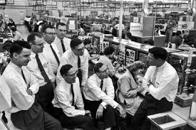
IBM needed advanced silicon transistors for a navigational computer. Texas Instruments had already provided samples, but they could not meet the required specifications. Noyce and a colleague traveled to IBM’s facility in upstate New York, where they were asked whether their barely established company could supply a hundred.
IBM은 항법 장치 컴퓨터에 사용할 첨단 실리콘 트랜지스터가 필요했습니다. 텍사스 인스트루먼트(Texas Instruments)가 이미 샘플을 제공했지만, 요구되는 사양을 충족하지 못하고 있었습니다. 노이스와 동료 한 명은 뉴욕주 북부에 있는 IBM 시설을 방문했고, 그곳에서 이제 막 설립된 그 회사가 트랜지스터 100개를 공급할 수 있는지 질문을 받았습니다.
Noyce’s answer was audacious: “Sure. We can do that.”
노이스의 대답은 대담했습니다. "그럼요. 할 수 있습니다."
There was one problem. Fairchild had not yet made a single transistor.
문제는 하나 있었습니다. 페어차일드는 아직 트랜지스터를 단 한 개도 만들지 못한 상태였습니다.
Noyce organized two parallel development efforts, increasing the odds that one would succeed. Five months after the company was founded, Fairchild delivered the hundred transistors on schedule.
노이스는 두 가지 개발 노력을 병행하여 성공 확률을 높였습니다. 회사가 설립된 지 5개월 후, 페어차일드는 약속된 일정에 맞춰 100개의 트랜지스터를 납품했습니다.
At the Wescon trade show the following month, the founders discovered that Fairchild had the only double-diffused silicon mesa transistors on the market. “We scooped the industry!” Noyce exulted afterward.
다음 달 열린 웨스콘(Wescon) 무역 박람회에서 창업자들은 페어차일드가 시장에서 유일하게 이중 확산 실리콘 메사 트랜지스터를 보유하고 있다는사실을 발견했습니다. "우리가 업계를 선점했습니다!" 노이스는 나중에 기뻐하며 외쳤습니다.
But mesa transistors were difficult to manufacture reliably. Their exposed surfaces were particularly vulnerable to contamination.
하지만 메사 트랜지스터는 안정적으로 제조하기가 까다로웠습니다. 표면이 그대로 노출되어 있어 오염에 특히 취약했기 때문입니다.
Another member of the Traitorous Eight, Swiss physicist Jean Hoerni, found a solution.
'반역의 8인' 중 또 다른 멤버인 스위스 출신의 물리학자 장 회르니(Jean Hoerni)가 해결책을 찾아냈습니다.
Hoerni developed what became known as the planar process, leaving a protective layer of silicon dioxide over the surface of the transistor. The technique made silicon devices far more robust and opened a path toward reliable, high-volume manufacturing.
회르니는 트랜지스터 표면 위에 이산화규소 보호막을 남겨두는, 이른바 '평면 공정(planar process)'을 개발했습니다. 이 기술은 실리콘 소자를 훨씬 더 튼튼하게 만들었으며, 신뢰성 높은 대량 생산으로 가는 길을 열어주었습니다.
In one memorable demonstration reported in Leslie Berlin’s biography of Noyce, Hoerni spat directly onto an unpackaged transistor. Contamination that could have ruined a mesa transistor left his planar device unharmed. It was a remarkable advance in making transistors.
레슬리 벌린(Leslie Berlin)이 쓴 노이스의 전기에 기록된 한 기억에 남는 시연에서, 회르니는 포장되지 않은 트랜지스터 위에 직접 침을 뱉었습니다. 메사 트랜지스터라면 망가뜨렸을 오염 물질에도 그의 평면 소자는 아무런 해를 입지 않았습니다. 이는 트랜지스터 제조 역사상 놀라운 발전이었습니다.
Noyce would soon realize that the planar process could be used to make something much more revolutionary.
노이스는 평면 공정을 이용해 훨씬 더 혁신적인 무언가를 만들 수 있음을 곧 깨닫게 됩니다.
The Revolutionary Idea That Almost Stayed in a Drawer
Fairchild’s patent attorney, John Ralls, had been working with Jean Hoerni on protecting the planar-process inventions. As head of R&D, Noyce was involved in those discussions, and Ralls challenged him to think more broadly about what else the technology might make possible. Noyce later credited that question with helping stimulate his thinking.
페어차일드의 특허 변호사인 존 롤스(John Ralls)는 장 회르니와 함께 평면 공정 관련 발명을 보호하는 작업을 진행하고 있었습니다. 연구개발(R&D) 책임자였던 노이스도 그 논의들에 참여하고 있었는데, 롤스는 그에게 이 기술이 또 무엇을 가능하게 할 수 있을지 더 넓은 시각으로 생각해 보라고 도발적인 질문을 던졌습니다. 노이스는 나중에 자신의 사고를 자극하는 데 그 질문이 큰 도움이 되었다고 회상했습니다.
His insight was deceptively simple.
그의 통찰은 겉보기엔 단순해 보였습니다.
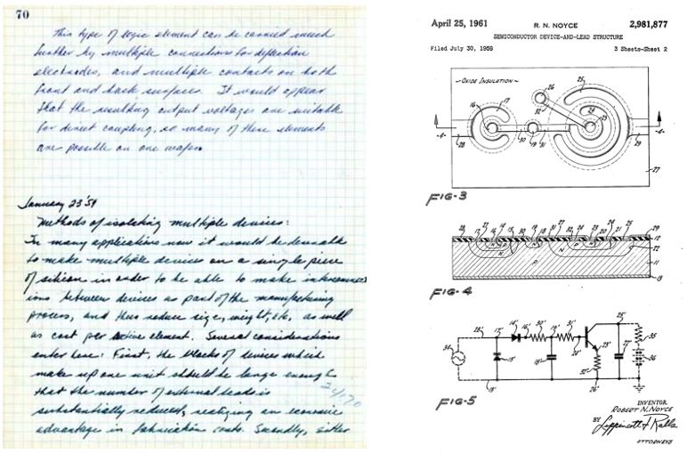
If multiple transistors and other components could be fabricated on the same piece of silicon using Hoerni’s planar process, why not connect them electrically by depositing and patterning metal interconnections directly on top of the insulating oxide layer? The individual components could be electrically isolated from one another using reverse-biased p-n junctions.
회르니의 평면 공정을 이용해 여러 개의 트랜지스터와 기타 부품을 동일한 실리콘 조각 위에 제조할 수 있다면, 절연성 산화막 바로 위에 금속 상호 연결(interconnections)을 직접 증착하고 패터닝하여 전기적으로 연결하면 어떨까요? 개별 부품들은 역방향 바이어스 p-n 접합을 사용해 서로 전기적으로 격리할 수 있을 것이었습니다.
The result would be an entire electronic circuit fabricated as a single monolithic chip.
그 결과는 단일한 모놀리식 칩으로 제조된 전체 전자 회로가 될 터였습니다.
Noyce recorded the idea in his notebook in January 1959.
노이스는 1959년 1월 자신의 공책에 이 아이디어를 기록했습니다.
And then, remarkably, amid other pressing priorities at Fairchild, it sat in his drawer for months.
그리고 놀랍게도, 페어차일드에서 처리해야 할 다른 시급한 현안들에 밀려 이 아이디어는 몇 달 동안 그의 서랍 속에 처박혀 있었습니다.
Meanwhile, Texas Instruments had been pursuing a similar goal. Jack Kilby had demonstrated that multiple electronic components could be fabricated from a single piece of semiconductor material, and in 1959 TI publicly announced what it called its “solid circuit.” But Kilby’s device connected its components with external “flying wires”—an approach that could not be scaled to the much higher levels of integration that would eventually be required.
한편 텍사스 인스트루먼트(TI) 역시 비슷한 목표를 추구하고 있었습니다. 잭 킬비(Jack Kilby)는 여러 개의 전자 부품이 단일 반도체 소재 조각에서 제조될 수 있음을 시연했고, 1959년 TI는 이른바 "솔리드 서킷(solid circuit)"을 공개적으로 발표했습니다. 하지만 킬비의 장치는 부품들을 외부의 "공중 배선(flying wires)"으로 연결했는데, 이는 결국 요구될 훨씬 더 높은 수준의 집적도로 확장할 수 없는 방식이었습니다.
As reported in the documentary Silicon Valley, a TI representative encountered then-Fairchild salesman Jerry Sanders at an industry conference and told him, “We’re going to crush you guys!”
다큐멘터리 《실리콘밸리》에 보도된 바와 같이, 한 TI 대표가 업계 컨퍼런스에서 당시 페어차일드의 영업사원이던 제리샌더스(Jerry Sanders)를 만나 이렇게 말했습니다. "우리가 너희들을 짓밟아 버릴 거야!"
That got Fairchild’s attention.
이 말은 페어차일드의 정신을 번쩍 차리게 만들었습니다.
Noyce’s concept had been developed independently of Kilby’s, but it offered a crucial advantage. By combining Hoerni’s planar process with p-n junction isolation and patterned metal interconnections on the oxide surface, it provided a practical architecture for manufacturing monolithic integrated circuits. The interconnections could now be fabricated along with the devices themselves rather than added individually with external wires. This directly tackled the “tyranny of numbers” problem and opened the way to ever-higher levels of integration.
노이스의 개념은 킬비의 것과 독립적으로 개발되었지만, 결정적인 우위를 지니고 있었습니다. 회르니의 평면 공정과 p-n 접합 격리, 그리고 산화물 표면의 패턴화된 금속 상호 연결을 결합함으로써, 모놀리식 집적회로를 제조하기 위한 실용적인 아키텍처를 제공했던 것입니다. 이제 상호 연결은 외부 와이어를 하나씩 덧붙이는 방식이 아니라 장치 자체와 함께 제조될 수 있게 되었습니다. 이는 '숫자의 횡포(tyranny of numbers)' 문제를 직접적으로 해결하고, 더 높은 수준의 집적도로 나아가는 길을 열어주었습니다.
Now Fairchild had to turn the concept into reality.
이제 페어차일드는 이 개념을 현실로 바꾸어야 했습니다.
Noyce pushed Jay Last and his team to move quickly enough to build a prototype IC and “show the flag” at the upcoming Wescon electronics show. Their early demonstration was crude, but it signaled that Fairchild was in the race. Last’s team then undertook the challenging work of turning Noyce’s concept into working monolithic circuits, eventually leading to Fairchild’s Micrologic devices and the commercialization of the silicon integrated circuit.
노이스는 제이 라스트(Jay Last)와 그의 팀을 독려하여 시제품 IC를 제작하고 다가오는 웨스콘(Wescon) 전자 박람회에서 "깃발을 꽂을(show the flag)" 수 있도록 충분히 빠른 속도로 움직이게 했습니다. 그들의 초기 시연은 조잡했지만, 페어차일드가 이 경쟁에 뛰어들었음을 알리는 신호탄이었습니다. 이후 라스트의 팀은 노이스의 개념을 작동하는 모놀리식 회로로 탈바꿈시키는 어려운 과업에 착수했고, 이는 결국 페어차일드의 마이크로로직(Micrologic) 소자와 실리콘 집적회로의 상용화로 이어졌습니다.
The chain of events leading to the development of the IC is striking: Hoerni’s manufacturing breakthrough, a patent attorney’s provocative question, Noyce’s conceptual leap, competitive pressure from Texas Instruments—and the engineering effort required to turn an idea into a manufacturable product.
IC 개발로 이어진 일련의 사건들은 매우 인상적입니다. 회르니의 제조상 돌파구, 특허 변호사의 도발적인 질문, 노이스의 개념적 도약, 텍사스 인스트루먼트의 경쟁 압력, 그리고 아이디어를 제조 가능한 제품으로 구체화하는 데 필요한 엔지니어링의 노력까지 말입니다.
It was precisely this unlikely sequence of invention, competition and human decision-making that made the episode such a compelling one to recreate in The Compass.
《더 컴퍼스》에서 이 에피소드를 재현하는 것이 그토록 매력적이었던 이유는 바로 이러한 발명, 경쟁, 그리고 인간의 의사결정이 빚어낸 묘한 우연의 연속 때문이었습니다.
From Invention to Commercialization
Inventing the IC was only part of the challenge. The semiconductor industry also had to develop the technologies and business models needed to manufacture chips in enormous quantities at steadily falling prices.
IC를 발명하는 것은 과제의 일부분에 불과했습니다. 반도체 산업은 또한 꾸준히 하락하는 가격으로 칩을 대량 생산하는 데 필요한 기술과 비즈니스 모델을 개발해야 했습니다.
Noyce played a role there as well.
노이스는 그 분야에서도 역할을 담당했습니다.
Fairchild engineers needed a way to reproduce microscopic patterns repeatedly across silicon wafers. Resourceful and hands-on as ever, Noyce helped build an early step-and-repeat photolithography system using matched 16mm lenses acquired from a local camera shop to print the fine patterns needed to fabricate integrated circuits—an ingenious precursor to the extraordinarily sophisticated lithography systems on which modern chipmaking depends.
페어차일드 엔지니어들은 실리콘 웨이퍼 전반에 걸쳐 미세한 패턴을 반복적으로 재현할 수 있는 방법이 필요했습니다. 언제나 그렇듯 재치 있고 직접 손으로 만드는 것을 즐겼던 노이스는 집적회로 제조에 필요한 미세 패턴을 인쇄하기 위해, 지역 카메라점에서 구입한 16mm 렌즈를 맞춤 조합하여 초기형 스텝 앤드 리피트(step-and-repeat) 포토리소그래피 시스템을 제작하는 것을 도왔습니다. 이는 현대 반도체 제조가 의존하고 있는 엄청나게 정교한 리소그래피 시스템의 독창적인 선구자였습니다.
Noyce also understood early that semiconductor manufacturing would become global. In the early 1960s, he sent Fairchild cofounder Julius Blank and manufacturing chief Charlie Sporck to investigate Hong Kong as a location for assembly. Their trip led Fairchild to establish a major operation there—an early milestone in the globalization of semiconductor manufacturing.
노이스는 또한 반도체 제조가 글로벌화될 것이라는 점을 일찍이 직감했습니다. 1960년대 초, 그는 페어차일드의 공동 창업자 줄리어스 블랭크(Julius Blank)와 제조 총괄 찰리 스포크(Charlie Sporck)를 홍콩으로 보내 조립 공장 부지를 조사하도록 했습니다. 그들의 여행 덕분에 페어차일드는 그곳에 대규모 사업장을 설립하게 되었는데, 이는 반도체 제조 글로벌화의 초기 이정표였습니다.
But perhaps Noyce’s most counterintuitive innovation involved price.
하지만 노이스의 가장 직관에 반하는 혁신은 아마도 '가격'과 관련이 있었을 것입니다.
In 1964, he made a startling decision: Fairchild would sell some of its low-end integrated circuits for less than they cost the company to manufacture.
1964년, 그는 놀라운 결정을 내렸습니다. 페어차일드가 자사의 보급형 집적회로 중 일부를 제조 원가보다 더 낮은 가격에 판매하기로 한 것입니다.
The logic was audacious: lower prices would increase demand; greater volume and technological progress would improve manufacturing yields and reduce unit costs; falling costs would stimulate still more demand.
그 논리는 대담했습니다. 가격이 낮아지면 수요가 늘어날 것이고, 물량 증대와 기술 진보는 제조 수율을 향상시키며 단위당 원가를 낮출 것이며, 하락하는 원가는 더 많은 수요를 자극할 것이라는 점이었습니다.
In 1965, Noyce pushed the strategy even further. At a major industry conference, he stunned the audience—and even some of his own colleagues—by announcing that Fairchild would price its major integrated-circuit products at one dollar apiece.
1965년, 노이스는 이 전략을 한 단계 더 밀어붙였습니다. 대규모 업계 컨퍼런스에서 그는 페어차일드의 주요 집적회로 제품 가격을 개당 1달러로 책정하겠다고 발표하여 청중과 심지어 자신의 동료들까지 경악게 했습니다.
Gordon Moore later called Noyce’s anticipatory pricing strategy an “invention” as important to the semiconductor industry as the integrated circuit itself. By deliberately pricing ahead of the cost curve, Fairchild could create the volume that would ultimately make those seemingly uneconomic prices profitable.
고든 무어는 나중에 노이스의 선제적 가격 책정 전략을 반도체 산업에 있어 집적회로 그 자체만큼이나 중요한 "발명"이라고 평가했습니다. 비용 곡선보다 의도적으로 앞서 가격을 책정함으로써, 페어차일드는 겉보기엔 채산성이 없어 보이던 가격을 마침내 수익성 있게 만들어 줄 수요를 창출해 낼 수 있었습니다.
That same year, Moore published his famous article in Electronics magazine observing that the number of components that could economically be placed on an integrated circuit was increasing exponentially. What would later become known as Moore’s Law captured the technological and economic trajectory that would drive the semiconductor industry for decades.
바로 그해, 무어는 《전자(Electronics)》 매거진에 집적회로에 경제적으로 실을 수 있는 부품의 수가 지수 함수적으로 증가하고 있다고 언급한 유명한 글을 기고했습니다. 나중에 '무어의 법칙'으로 알려지게 된 이 개념은 수십 년 동안 반도체 산업을 이끌어갈 기술적, 경제적 궤적을 포착해 냈습니다.
Moore put that exponential trajectory on a graph. Noyce’s pricing strategy was already betting that falling costs and rising volumes would help make it possible.
무어는 그 지수 함수적 궤적을 그래프 위에 그려 넣었습니다. 반면 노이스의 가격 책정 전략은 하락하는 원가와 상승하는 물량이 그 궤적을 현실화하는 데 기여할 것임을 이미 확신하고 있었습니다.
Building Intel—and a New Kind of Company
By the late 1960s, Fairchild Semiconductor had become one of America’s most important technology companies. But friction with its East Coast parent was growing, and Noyce became increasingly frustrated.
1960년대 후반에 이르러 페어차일드 반도체는 미국에서 가장 중요한 기술 기업 중 하나로 성장했습니다. 그러나 동부의 모회사와의 마찰이 커졌고, 노이스는 점점 더 좌절감을 느꼈습니다.
In 1968, he decided to leave.
1968년, 그는 회사를 떠나기로 결심했습니다.
Gordon Moore dropped by Noyce’s house one spring morning while Noyce was mowing his lawn. The two discussed starting another company.
어느 봄날 아침, 고든 무어는 노이스가 잔디를 깎고 있던 그의 집에 들렀습니다. 두 사람은 새로운 회사를 시작하는 것에 대해 논의했습니다.
It was an echo of 1957.
그것은 1957년의 메아리였습니다.
Then, Noyce had been persuaded to join seven colleagues leaving Shockley. Eleven years later, he and Moore were walking away from the company they had helped create.
당시 노이스는 쇼클리를 떠나는 7명의 동료에 합류해 달라고 설득을 받았었습니다. 11년이 지난 후, 그와 무어는 자신들이 직접 세우는 데 기여했던 회사를 떠나고 있었습니다.
They envisioned a company initially focused on semiconductor memory and built around continuous technological innovation. Staying on the exponential trajectory Moore had identified three years earlier would be a guiding principle.
그들은 초기에는 반도체 메모리에 집중하고 지속적인 기술 혁신을 중심으로 구축되는 회사를 구상했습니다. 3년 전에 무어가 파악했던 지수 함수적 궤적을 계속 유지하는 것이 지침 원리가 될 터였습니다.
With financing again provided by Arthur Rock, the new venture was incorporated on July 18, 1968. Noyce and Moore initially called it NM Electronics before settling on Intel.
아서 록이 다시 한번 자금 조달을 맡은 가운데, 새로운 벤처 기업은 1968년 7월 18일에 법인화되었습니다. 노이스와 무어는 인텔(Intel)로 확정하기 전에 처음에는 이 회사를 'NM 일렉트로닉스(NM Electronics)'라고 불렀습니다.
But they were creating more than another semiconductor company. Noyce helped give Intel a distinctly different culture.
그러나 그들이 만들고 있던 것은 또 하나의 반도체 그 이상이었습니다. 노이스는 인텔에 완전히 다른 문화가 자리 잡도록 기여했습니다.
Traditional corporations of the era were hierarchical, with private executive offices, privileges and visible symbols of rank. Noyce preferred informality and accessibility. He believed authority should come from ideas and competence rather than titles.
당시의 전통적인 기업들은 위계질서가 엄격했으며, 전용 임원실과 특권, 그리고 직급을 드러내는 가시적인 상징들이 존재했습니다. 반면 노이스는 비식전적인 분위기와 접근성을 선호했습니다. 그는 권력이 직함이 아니라 아이디어와 역량에서 나와야 한다고 믿었습니다.
At Intel, Noyce famously worked in a cubicle rather than an executive suite, encouraged direct communication with the executive team and helped extend stock ownership more broadly among employees. In Tom Wolfe’s celebrated 1983 Esquire portrait of Noyce, he described this emerging Silicon Valley culture as a rejection of the “feudal” conventions of traditional corporate America.
인텔에서 노이스는 임원실 대신 큐비클에서 일하고, 경영진과의 직접적인 소통을 장려했으며, 직원들 사이에서 주식 소유가 더 폭넓게 이루어지도록 도왔다는 일화로 유명합니다. 톰 울프(Tom Wolfe)가 1983년 《에스콰이어(Esquire)》지에 기고한 노이스에 대한 유명한 인물평에서, 그는 이러한 신흥 실리콘밸리 문화를 전통적인 미국 기업의 "봉건적" 관습에 대한 거부로 묘사했습니다.
That culture would become characteristic of much of Silicon Valley. Noyce was helping create not merely new semiconductor products, but a new model for a technology company.
이러한 문화는 실리콘밸리 대다수의 특징으로 자리 잡게 되었습니다. 노이스는 단순히 새로운 반도체 제품을 만드는 것을 넘어, 기술 기업을 위한 새로운 모델을 만들어내고 있었습니다.
And Intel was about to face another technological turning point.
그리고 인텔은 또 다른 기술적 전환점을 마주하게 되었습니다.
The Idea Intel Almost Didn’t Pursue
In 1969, Japanese calculator manufacturer Busicom asked Intel to develop a complex family of custom chips for a new calculator.
1969년, 일본의 계산기 제조업체인 부시콤(Busicom)은 인텔에 신형 계산기를 위한 복잡한 맞춤형 칩 세트 개발을 의뢰했습니다.
Intel engineer Ted Hoff studied the proposal and saw another possibility. Rather than build many specialized logic chips, why not create a general-purpose processor whose functions could be changed through programming?
인텔의 엔지니어 테드 호프(Ted Hoff)는 이 제안을 검토하다가 또 다른 가능성을 발견했습니다. 수많은 특화된 로직 칩을 만드는 대신, 프로그래밍을 통해 기능을 변경할 수 있는 범용 프로세서를 만들면 어떨까 하는 것이었습니다.
It was the fundamental concept behind the microprocessor.
이것이 바로 마이크로프로세서의 근본적인 개념이었습니다.
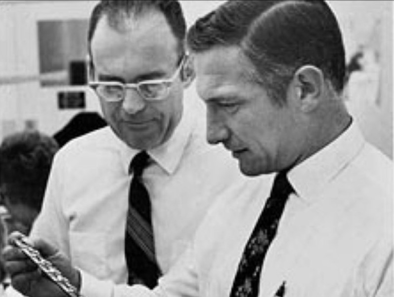
Hoff brought the idea to Noyce, who immediately saw its potential. But Intel was a young company under financial pressure, struggling to bring its 1103 DRAM into reliable production. Resources were stretched, and Andy Grove initially resisted diverting people to a speculative processor project.
호프는 이 아이디어를 노이스에게 가져갔고, 노이스는 즉시 그 잠재력을 알아보았습니다. 하지만 인텔은 1103 DRAM의 안정적인 양산에 어려움을 겪고 있던 재정적 압박 속의 신생 기업이었습니다. 자원은 턱없이 부족했고, 앤디 그로브(Andy Grove)는 투기적인 성격의 프로세서 프로젝트에 인력을 차출하는 것에 처음에는 난색을 표했습니다.
Noyce gave Hoff the freedom to keep pursuing it.
그럼에도 노이스는 호프에게 계속 연구를 진행할 수 있는 자유를 주었습니다.
Turning the concept into working silicon was another challenge. Noyce enlisted Grove in recruiting Federico Faggin from Fairchild, and Faggin led the difficult implementation effort that ultimately produced a working processor.
그 개념을 실제로 작동하는 실리콘으로 구현하는 것은 또 다른 과제였습니다. 노이스는 앤디 그로브와 함께 페어차일드에서 페데리코 파진(Federico Faggin)을 영입하는 데 힘을 보탰고, 파진이 주도한 힘겨운 구현 작업 끝에 마침내 작동하는 프로세서가 탄생했습니다.
One obstacle remained: Busicom owned the rights.
하지만 한 가지 걸림돌이 남아있었습니다. 권리를 부시콤이 소유하고 있었던 것입니다.
When the Japanese company’s financial difficulties led it to renegotiate its agreement with Intel, Noyce seized the opportunity. Intel returned Busicom’s $60,000 development investment in exchange for the rights to sell the processor for applications beyond calculators.
일본 회사의 재정난으로 인해 부시콤이 인텔과의 계약 재협상을 요구했을 때, 노이스는 이 기회를 놓치지 않았습니다. 인텔은 계산기 외의 다른 용도로 프로세서를 판매할 수 있는 권리를 넘겨받는 조건으로 부시콤에 개발 투자금 6만 달러를 돌려주었습니다.
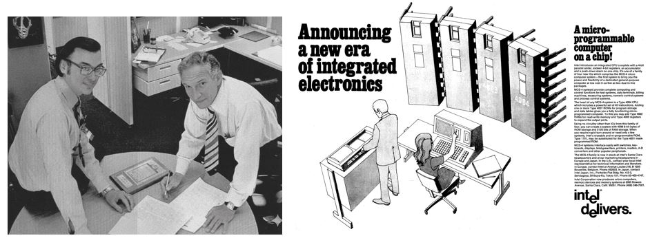
On November 15, 1971, Intel announced the 4004 general-purpose programmable microprocessor to the world.
1971년 11월 15일, 인텔은 세계 최초의 범용 프로그래밍 가능 마이크로프로세서인 4004를 세상에 발표했습니다.
The full story of the 4004’s development—and the remarkable team behind it—is one I explore in greater detail in my novel The Compass. But Noyce’s role highlights a different kind of contribution.
4004 개발의 전체적인 비화와 그 이면의 놀라운 팀에 대해서는 제 소설 《더 컴퍼스(The Compass)》에서 더욱 자세히 다루고 있습니다. 하지만 여기서 노이스의 역할은 전혀 다른 차원의 기여를 보여줍니다.
He did not invent the microprocessor. He recognized a potentially transformative idea, gave it room to develop when his company had plenty of reasons to focus elsewhere, brought in the talent needed to make it real, and ensured that Intel could take it to the broader market.
그는 마이크로세서를 직접 발명하지는 않았습니다. 대신 회사가 다른 곳에 집중해야 할 타당한 이유가 많았던 상황에서도 세상을 바꿀 잠재력을 가진 아이디어를 알아보고, 그것이 발전할 수 있는 여유를 주었으며, 현실화하는 데 필요한 인재를 영입하고, 인텔이 더 넓은 시장으로 나아갈 수 있도록 발판을 마련해 주었습니다.
1971: The Year the Pieces Came Together
The 4004 was only one part of an extraordinary convergence.
4004는 놀라운 융합의 한 조각에 불과했습니다.
Intel had introduced the 1103 DRAM in 1970. After stubborn early manufacturing and reliability problems were overcome, by the end of 1971 it had become the world’s largest-selling semiconductor device.
인텔은 1970년에 1103 DRAM을 출시했습니다. 완강했던 초기 제조 및 신뢰성 문제가 극복된 후, 1971년 말 무렵 이 제품은 세계에서 가장 많이 팔리는 반도체 소자가 되었습니다.
In 1971, Intel also introduced the 1702 EPROM, the first commercially available erasable programmable read-only memory—a practical form of nonvolatile semiconductor memory.
또한 인텔은 1971년에 상용화된 최초의 지우고 쓸 수 있는 프로그래밍 가능 읽기 전용 메모리(EPROM)인 1702 EPROM을 선보였습니다. 이는 실용적인 형태의 비휘발성 반도체 메모리였습니다.
Processor. Working memory. Nonvolatile memory.
Three fundamental building blocks of modern digital electronics had come together at one young Silicon Valley company. It is why semiconductor veteran John East, writing in SemiWiki, has called 1971 “The Year Intel Changed the World.”
현대 디지털 전자기기의 세 가지 근본적인 구성 요소가 실리콘밸리의 한 신생 기업에서 하나로 모인 것입니다. 반도체 베테랑인 존 이스트(John East)가 세미위키(SemiWiki)에 기고하며 1971년을 “인텔이 세상을 바꾼 해”라고 부른 이유가 바로 여기에 있습니다.
And 1971 brought one more historical coincidence.
그리고 1971년에는 역사적인 우연이 한 가지 더 겹쳤습니다.
On January 11, journalist Don Hoefler began a three-part series in Electronic News under the headline “Silicon Valley U.S.A.” His articles helped popularize the iconic name that would soon become synonymous with the technology industry itself.
1월 11일, 언론인 돈 호플러(Don Hoefler)가 《전자 뉴스(Electronic News)》에 “실리콘밸리 미국(Silicon Valley U.S.A.)”이라는 헤드라인으로 3부작 연재 기사를 시작했습니다. 그의 기사는 머지않아 기술 산업 그 자체의 대명사가 될 상징적인 이름을 대중화하는 데 기여했습니다.
The industry had spent more than a decade creating Silicon Valley.
업계는 10년 넘는 시간을 들여 실리콘밸리를 만들어냈습니다.
Now the world had a name for it.
이제 세상은 그곳을 부를 이름을 갖게 되었습니다.
None of It Was Inevitable
Looking backward, Silicon Valley can seem like an inevitable progression: transistor to Fairchild, Fairchild to the integrated circuit, integrated circuit to Intel, Intel to the microprocessor.
돌이켜보면 실리콘밸리의 탄생은 마치 필연적인 수순처럼 보일 수 있습니다. 트랜지스터에서 페어차일드로, 페어차일드에서 집적회로로, 집적회로에서 인텔로, 그리고 인텔에서 마이크로프로세서로 이어지는 흐름 말입니다.
But viewed up close, none of it looks inevitable.
하지만 가까이 들여다보면 그 무엇도 필연적인 것은 없었습니다.
The transistor monographs from Bell Labs might never have found their way to a small college in Iowa and sparked the curiosity of a young Robert Noyce. Noyce could have stayed with Shockley. Sherman Fairchild could have joined the dozens of others who had already said no. Noyce could have told IBM that his fledgling company was not yet ready to promise a hundred demanding silicon transistors when it had not built even one. His integrated-circuit idea could have remained in his drawer. Fairchild could have priced ICs conventionally. Noyce could have remained at Fairchild. Intel could have abandoned Hoff’s processor.
벨 연구소의 트랜지스터 기술 모노그래프가 아이오와주의 작은 대학에 전해져 젊은 로버트 노이스의 호기심을 자극하지 못했을 수도 있습니다. 노이스는 쇼클리 곁에 계속 남아있을 수도 있었습니다. 셔먼 페어차일드는 이미 거절 의사를 밝혔던 수많은 다른 투자자들처럼 투자를 마다했을 수도 있습니다. 노이스는 단 한 개도 만들어본 적 없는 까다로운 실리콘 트랜지스터 100개를 공급하겠다고 IBM에 호기롭게 약속하지 않을 수도 있었습니다. 그의 집적회로 아이디어는 영원히 서랍 속에 묵혀 있었을지도 모릅니다. 페어차일드는 IC를 통상적인 방식으로 가격 책정했을 수 있습니다. 노이스는 페어차일드에 계속 남아있을 수도 있었습니다. 인텔은 호프의 프로세서 개발을 포기했을지도 모릅니다.
Noyce did not shape these events alone. Hoerni, Moore, Rock, Last, Hoff, Faggin, Grove and many others made indispensable contributions. But again and again, Noyce was there at the critical juncture—recognizing the possibility, taking the risk or helping turn an idea into reality.
물론 노이스 혼자서 이 모든 역사를 빚어낸 것은 아닙니다. 회르니, 무어, 록, 라스트, 호프, 파진, 그로브를 비롯한 수많은 이들이 대체 불가능한 기여를 했습니다. 하지만 노이스는 결정적인 순간마다 그 자리에 있었습니다. 가능성을 알아보고, 위험을 감수하며, 아이디어를 현실로 바꾸어 놓는 그 중심에 항상 그가 있었습니다.
That is why, when I wrote The Compass, I chose Noyce as one of its three central historical figures, alongside Albert Einstein and Steve Jobs. His story is not simply one of invention, but of also recognizing possibilities—and acting on them at moments when the outcome was far from certain.
제가 소설 《더 컴퍼스(The Compass)》를 집필할 때 알베르트 아인슈타인, 스티브 잡스와 함께 로버트 노이스를 세 명의 핵심 역사적 인물 중 한 명으로 선택한 이유가 바로 여기에 있습니다. 그의 이야기는 단순한 발명의 역사가 아닙니다. 그것은 가능성을 알아보고, 결과가 전혀 확실하지 않은 순간에 과감히 행동으로 옮겼던 사람의 이야기입니다.
Silicon Valley was built through breakthroughs, risks and choices. At each of its pivotal moments, someone had to make a critical decision.
실리콘밸리는 수많은 돌파구와 위험, 그리고 선택을 통해 구축되었습니다. 그 모든 중대한 순간마다 누군가는 결단을 내려야만 했습니다.
Nearly every time, that someone was Robert Noyce.
그리고 거의 모든 그 순간에, 그 누군가는 바로 로버트 노이스였습니다.
About the Author
Sunil Mehta has spent more than forty years in Silicon Valley in technical and leadership roles at companies such as Intel and AMD. His recently published debut novel, The Compass, blends historical fact with imaginative storytelling to explore the lives and pivotal contributions of Albert Einstein, Robert Noyce and Steve Jobs against the backdrop of the origins of Silicon Valley.
수닐 메타(Sunil Mehta)는 인텔(Intel)과 AMD 등의 기업에서 기술 및 리더십 역할을 맡으며 실리콘밸리에서 40년 이상 종사해 왔습니다. 최근 출간된 그의 데뷔 소설 《더 컴퍼스(The Compass)》는 실리콘밸리의 탄생을 배경으로, 역사적 사실과 상상력이 가미된 스토리텔링을 결합하여 알베르트 아인슈타인, 로버트 노이스, 스티브 잡스의 삶과 결정적인 기여를 조명하고 있습니다.



