The Wafer Is the New Battleground: Soitec CPO René Jonker on Building AI from the Substrate Up
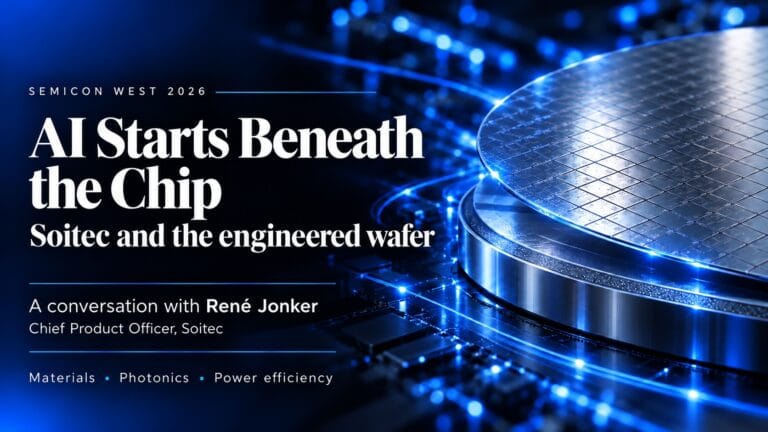
Most of the AI conversation stops at the chip. At SEMICON West 2026 I sat down with René Jonker, Chief Product Officer of Soitec, to talk about what sits underneath it.
대부분의 인공지능(AI) 관련 대화는 칩에서 멈춥니다. 2026년 SEMICON West에서 저는 소이텍(Soitec)의 최고제품책임자(CPO)인 르네 욘커(René Jonker)를 만나 그 이면에 무엇이 있는지에 대해 이야기를 나누었습니다.
Ask an engineer where AI performance comes from and you will hear about process nodes, dataflow, HBM stacks and interconnect fabrics. Rarely about the wafer. Yet a Grenoble company that most people outside the industry have never heard of has quietly built its business on a simple idea: if you engineer the right properties into the starting material, the foundry does not have to fight physics later.
엔지니어에게 AI 성능이 어디서 오는지 물어보면 공정 노드(process node), 데이터플로우, HBM 스택, 인터커넥트 패브릭에 대한 이야기를 듣게 됩니다. 웨이퍼에 대한 이야기는 거의 나오지 않습니다. 하지만 업계 외의 대부분 사람들이 들어본 적 없는 한 그르노블(Grenoble)의 회사는 아주 단순한 아이디어 위에 사업을 조용히 구축해 왔습니다. 즉, 시작 소재에 올바른 물성을 설계해 넣으면 파운드리가 나중에 물리학과 싸울 필요가 없어진다는 것입니다.
The market has noticed. Soitec trades on Euronext Paris, and an investor who put $100 into its stock in January 2026 was holding more than $600 by early October. So I opened with the obvious question: what is the secret sauce?
시장은 이를 알아차렸습니다. 소이텍은 유로넥스트 파리(Euronext Paris)에 상장되어 있으며, 2026년 1월에 이 회사 주식에 100달러를 투자한 투자자는 10월 초 무렵 600달러 이상을 보유하게 되었습니다. 그래서 저는 뻔한 질문으로 인터뷰를 시작했습니다. 바로 “성공의 비결(secret sauce)이 무엇인가?”라는 것입니다.
A thirty-year bet on one cut
Soitec was spun out of CEA-Leti in 1992 to commercialize Smart Cut, a process that uses ion implantation and wafer bonding to slice a layer of monocrystalline silicon only nanometers thick and transfer it onto an insulating substrate. The result is silicon-on-insulator (SoI), and the name of the company says the rest.
소이텍은 이온 주입과 웨이퍼 본딩 기술을 이용해 나노미터 두께에 불과한 단결정 실리콘 층을 잘라내어 절연 기판 위로 전이하는 공정인 ‘스마트 컷(Smart Cut)’을 상용화하기 위해 1992년 CEA-Leti에서 분사(spin-out)해 나왔습니다. 그 결과물이 바로 실리콘 온 인슐레이터(SoI)이며, 회사의 이름이 나머지를 말해줍니다.
The road was not straight. Early growth came from SOI supply deals with AMD and IBM for high-performance computing. Dependence on a few customers, and a detour into solar, brought turbulence in the 2000s. The 2010s brought the turnaround, when restructured leadership went back to the core and found its killer application: RF-SOI for smartphone front-end modules.
지나온 길이 순탄치만은 않았습니다. 초기 성장은 고성능 컴퓨팅을 위해 AMD와 IBM에 SOI 공급 계약을 따내며 이루어졌습니다. 소수의 고객에 대한 의존도와 태양광 사업으로의 외도는 2000년대에 혼란을 가져왔습니다. 2010년대에는 구조조정된 경영진이 핵심으로 회귀하여 스마트폰 프런트엔드 모듈용 RF-SOI라는 킬러 어플리케이션을 찾아내면서 반등을 맞이했습니다.
Soitec is neither a foundry nor a fabless designer. It sits at the very bottom of the value chain. Foundries and IDMs such as TSMC, GlobalFoundries, STMicroelectronics, Samsung Foundry and UMC buy its wafers as starting material. Fabless companies such as Qualcomm, Apple, Broadcom, MediaTek and NXP specify Soitec platforms in their designs, and the foundries follow.
소이텍은 파운드리도 아니고 팹리스 설계 회사도 아닙니다. 가치 측면의 맨 아래 바닥에 자리 잡고 있습니다. TSMC,글로벌파운드리(GlobalFoundries), ST마이크로일렉트로닉스(STMicroelectronics), 삼성 파운드리, UMC 같은 파운드리와 IDM들이 시작 소재로서 소이텍의 웨이퍼를 구매합니다. 퀄컴(Qualcomm), 애플(Apple), 브로드컴(Broadcom), 미디어텍(MediaTek), NXP 같은 팹리스 기업들이 설계 도면에 소이텍 플랫폼을 지정하면 파운드리들이 그에 따릅니다.
That position matters more every year. As transistor scaling runs into leakage, parasitic capacitance and thermal limits, bulk silicon becomes the bottleneck. A buried oxide layer under a thin film of silicon attacks those problems at the material level, often cutting power by 30 to 50 percent without a node shrink.
그 위치는 갈수록 중요해지고 있습니다. 트랜지스터 스케일링이 누설 전류, 기생 용량(parasitic capacitance), 열계계 한계에 부딪히면서 벌크 실리콘은 병목 현상이 됩니다. 얇은 실리콘 박막 아래에 위치한 매몰 산화막(buried oxide) 층은 소재 수준에서 이러한 문제들을 해결하며, 노드 축소 없이도 전력을 30%에서 50%까지 절감해 줍니다.
Built into the starting material
Jonker puts the formula in one sentence. “By providing a substrate, you can add properties to silicon at a very early stage. Rather than having a foundry do very complicated things to get similar performance, your starting material already has certain features built in.”
욘커는 이 공식을 한 문장으로 요약합니다. “기판을 제공함으로써, 여러분은 아주 초기 단계에서 실리콘에 속성을 더할 수 있습니다. 파운드리가 유사한 성능을 내기 위해 매우 복잡한 일들을 수행하게 만드는 대신, 시작소재가 이미 특정 기능들을 내장하고 있는 것입니다.”
RF-SOI is the proof. By eliminating the parasitics of bulk silicon, it displaced competing technologies in mobile front-end modules and turned Soitec from a small player into the dominant supplier. Today it sits in RF switches and low-noise amplifiers in practically every 5G phone and Wi-Fi module.
RF-SOI가 그 증거입니다. 벌크 실리콘의 기생 효과를 제거함으로써 모바일 프런트엔드 모듈 분야에서 경쟁 기술들을 밀어내고 소이텍을 소규모 플레이어에서 지배적인 공급업체로 탈바꿈시켰습니다. 오늘날 이 기술은 사실상 모든 5G 스마트폰과 와이파이(Wi-Fi) 모듈의 RF 스위치 및 저잡음 증폭기(LNA)에 탑재되어 있습니다.
“That’s a little bit behind us now,” Jonker says. What Soitec discovered is that the same toolbox can make many kinds of substrates. The company now runs five main technology platforms, each built to solve a problem that is hard to fix further down the chain.
“이제 그것은 우리에게 약간 과거의 일이 되었습니다.” 욘커는 말합니다. 소이텍이 발견한 것은 동일한 도구 상자(toolbox)로 다양한 종류의 기판을 만들 수 있다는 점이었습니다. 이 회사는 현재 5개의 주요 기술 플랫폼을 운영하고 있으며, 각 플랫폼은 공급망 하단에서 해결하기 어려운 문제를 해결하도록 설계되었습니다.
Light becomes the new gold
The platform carrying Soitec today is one it developed a decade ago: Photonics-SOI.
오늘날 소이텍을 이끌고 있는 플랫폼은 10년 전에 개발한 포토닉스 SOI(Photonics-SOI)입니다.
“It’s now seen as the new gold,” Jonker says. The AI build-out has created a new problem: connecting the clusters. Copper runs out of bandwidth, so traffic moves to fiber. But somewhere electrons must become photons, and that interface is where Photonics-SOI lives, letting designers build optical waveguides in a silicon-based infrastructure. It is driving Soitec’s business “with a very impressive growth rate,” and it underpins the co-packaged optics now coming into AI data centers.
“이것은 이제 새로운 금으로 여겨지고 있습니다.” 욘커의 말입니다. AI 인프라 구축은 클러스터들을 서로 연결해야 하는 새로운 문제를 만들어냈습니다. 구리는 대역폭이 한계에 달해 트래픽이 광섬유(fiber)로 이동하고 있습니다. 하지만 어딘가에서는 전자가 광자로 변환되어야 하며, 바로 그 인터페이스가 포토닉스 SOI가 존재하는 영역입니다. 이를 통해 설계자들은 실리콘 기반 인프라 안에 광 도파로(optical waveguide)를 구축할 수 있습니다. 이 기술은 “매우 인상적인 성장률”로 소이텍의 사업을 견인하고 있으며, 현재 AI 데이터 센터로 진입하고 있는 공동 패키지 광학(co-packaged optics)의 기반이 되고 있습니다.
Between RF-SOI, the past, and photonics, the present, sits a broad middle. FD-SOI, fully depleted SOI, cuts leakage and therefore the power of compute units, with back-biasing to trade speed against power on the fly. Automotive radar, IoT microcontrollers and edge devices use it. “I have a watch that has FD-SOI in it,” Jonker adds. Power-SOI handles high-voltage automotive and industrial circuits, and Piezoelectric-on-Insulator (POI) targets acoustic RF filters for 5G and 6G.
과거를 뜻하는 RF-SOI와 현재를 뜻하는 포토닉스 사이에는 넓은 중간 영역이 자리 잡고 있습니다. 완전 공핍형 SOI인 FD-SOI는 누설 전류를 줄여 컴퓨팅 유닛의 전력을 절감하며, 실시간으로 속도와 전력을 맞바꾸는 백바이어싱(back-biasing) 기능을 제공합니다. 오토모티브 레이더, 사물인터넷(IoT) 마이크로컨트롤러, 엣지 디바이스들이 이를 사용합니다. “제 시계에도 FD-SOI가 들어가 있습니다”라고 욘커는 덧붙입니다. 파워 SOI(Power-SOI)는 고전압 자동차 및 산업용 회로를 처리하며, 압전기판 온 인슐레이터(POI)는 5G 및 6G용 음향 RF 필터를 겨냥합니다.
Beyond silicon
The bigger shift, in Jonker’s view, is the role of materials itself. “Up until more recently, everything was silicon. Everybody talked about TSMC silicon technology.” A lot of compute is still “plain vanilla silicon,” he concedes. But demand is growing for highly specialized materials, from gallium nitride to silicon carbide, that enable features classical silicon cannot. “That will not stop. For me it is very clear: we will see more and more different kinds of materials.”
욘커의 시각에서 더 큰 변화는 소재 그 자체의 역할입니다. “최근까지만 해도 모든 것이 실리콘이었습니다. 모든 사람이 TSMC의 실리콘 기술에 대해 이야기했습니다.” 여전히 많은 컴퓨팅이 ‘순정 실리콘(plain vanilla silicon)’으로 이루어지고 있다는 점은 그도 인정합니다. 그러나 전통적인 실리콘이 구현할 수 없는 기능을 가능하게 해주는 갈륨 나이트라이드(GaN)부터 실리콘 카바이드(SiC)까지, 고도로 특화된 소재에 대한 수요가 증가하고 있습니다. “이것은 멈추지 않을 것입니다. 제게는 아주 명확합니다. 우리는 점점 더 다양한 종류의 소재들을 보게 될 것입니다.”
Soitec is positioning for it. SmartSiC reuses a single-crystal silicon carbide donor wafer many times over, bonding a thin layer onto a conductive base, which lowers the cost of SiC power devices for EV inverters. RF-GaN on insulator is in development for 6G power amplifiers and aerospace. And FD-SOI is moving to smaller geometries to serve energy-conscious on-device AI in phones and wearables.
소이텍은 이에 대비하고 있습니다. 스마트SiC(SmartSiC)는 단결정 실리콘 카바이드 도너 웨이퍼를 여러 번 재사용하여 얇은 층을 전도성 베이스에 본딩함으로써, 전기차 인버터용 SiC 전력 소자의 비용을 낮춥니다. 절연체 위의 RF-GaN(RF-GaN on insulator)은 6G 전력 증폭기와 항공우주 분야를 위해 개발 중입니다. 그리고 FD-SOI는 스마트폰과 웨어러블 기기에서 에너지 효율적인 온디바이스 AI를 지원하기 위해 더 미세한 기하학적 구조로 진화하고 있습니다.
Two kinds of competition
When I asked about competitors, Jonker cautioned that he would share only what he was allowed to. Then he drew a useful distinction.
경쟁사들에 대해 물었을 때, 욘커는 허용된 내용만 공유하겠다며 주의를 기울였습니다. 그러고 나서 그는 유용한 구분을 내려주었습니다.
Direct competition, meaning other suppliers of similar substrates, comes mostly from GlobalWafers, which “has or used to have access to our IP.” There is “a long story” there he chose not to retell, and he does not see them at Soitec’s level today.
유사한 기판의 다른 공급업체들을 의미하는 직접적인 경쟁은 주로 “당사의 IP에 접근할 수 있거나 접근했던” 글로벌웨이퍼스(GlobalWafers)로부터 옵니다. 거기에는 그가 다시 말하지 않기로 선택한 “긴 이야기”가 있으며, 그는 현재 글로벌웨이퍼스가 소이텍의 수준에 와 있다고 보지 않습니다.
The more interesting competition is between technologies. An FD-SOI customer could instead choose FinFET at TSMC. “FinFET technology is not super efficient in terms of power usage,” he notes, so a designer who wants to win on power has a reason to pick FD-SOI. The two are not identical, but the end customer has a choice.
더 흥미로운 경쟁은 기술 간의 경쟁입니다. FD-SOI 고객은 대신 TSMC의 핀펫(FinFET)을 선택할 수도 있습니다. “핀펫 기술은 전력 사용 관점에서 그리 슈퍼 효율적이지 않습니다”라고 그는 지적하며, 전력 측면에서 승리하기를 원하는 설계자에게는 FD-SOI를 선택할 이유가 생긴다고 말합니다. 둘이 완전히 동일하지는 않지만 최종 고객에게는 선택권이 있습니다.
Photonics has the same tension. Silicon is “an okay material” for waveguides. Indium phosphide is better on performance. But silicon wins on everything around it: “The whole industry is basically set up for silicon, and indium phosphide is a difficult material to begin with.”
포토닉스도 동일한 긴장 관계를 안고 있습니다. 실리콘은 도파로 관점에서 “쓸만한 소재”입니다. 인듐 인화물(Indium phosphide)은 성능 면에서 더 뛰어납니다. 하지만 실리콘은 그 주변의 모든 생태계에서 승리합니다. “전체 산업이 기본적으로 실리콘에 맞춰 세팅되어 있으며, 인듐 인화물은 애초에 다루기 어려운 소재이기 때문입니다.”
The view from the bottom of the stack
That last point sums up Soitec’s position. Its substrates rarely win on raw physics alone. They win because they bring a new property into a manufacturing world built for silicon, at the one point in the chain where it is cheapest to add.
마지막 요점은 소이텍의 위치를 잘 요약해 줍니다. 이들의 기판이 순수 물리학만으로 승리하는 경우는 드뭅니다. 실리콘을 위해 구축된 제조 세계에 새로운 속성을 불어넣어 주며, 그것도 체인에서 추가 비용이 가장 저렴한 바로 그 지점에서 속성을 더해주기 때문에 승리하는 것입니다.
For thirty years that was a niche story. In the AI era, where every watt and every bit moved between chips counts, the wafer is becoming a design decision. Jonker’s bet is that the materials list will only get longer, and that the company holding the cut will be there when it does.
30년 동안 그것은 틈새시장 이야기였습니다. 칩 간에 이동하는 모든 와트와 모든 비트가 중요한 AI 시대에, 웨이퍼는 이제 하나의 설계 결정 사항이 되고 있습니다. 욘커의 도박은 소재 리스트가 앞으로 더욱 길어질 것이며, 절단 기술을 쥐고 있는 회사가 바로 그 순간 그 자리에 있을 것이라는 점입니다.



