Why Advanced Chip Packaging Is Becoming a Design Problem
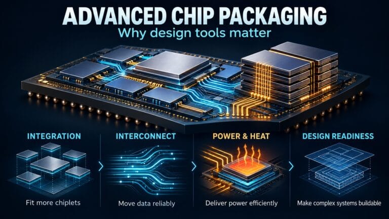
As chipmakers put more computing power into a single system, the challenge extends beyond making individual chips faster. They must connect multiple chips, memory stacks, power supplies, and sometimes optical components in a compact package. In the 2026 TSMC OIP Forum talk “Addressing Inter-Die Complexity for 3D Multi-Die Design by Synopsys / Arm”, TSMC describes how that growing complexity is changing the tools used to design chips. Physical layout, electrical performance, heat, and mechanical structure now have to be considered together.
칩 제조사들이 단일 시스템에 더 많은 연산 능력을 집어넣으면서, 개별 칩을 더 빠르게 만드는 것 이상의 과제가 대두되고 있습니다. 이들은 여러 개의 칩, 메모리 스택, 전원 공급 장치, 그리고 때로는 광학 부품까지 콤팩트한 패키지 하나에 연결해야 합니다. 2026 TSMC OIP 포럼에서 발표된 시놉시스(Synopsys)와 암(Arm)의 강연인 “Addressing Inter-Die Complexity for 3D Multi-Die Design”에서 TSMC는 이러한 복잡성 증가가 칩 설계 툴을 어떻게 변화시키고 있는지 설명합니다. 이제 물리적 레이아웃, 전기적 성능, 발열, 그리고 기계적 구조를 모두 함께 고려해야 합니다.
The first challenge is integration. Modern packages can place chiplets side by side and stack them vertically. Connections that pass through silicon, wiring tracks, and the spaces available for standard cells all follow different grids. If those grids are poorly aligned, a connection may block more usable space than necessary. TSMC describes adjusting connection placement to recover space for circuit cells. A small percentage gain can matter when repeated across a large design: it creates room for useful circuitry without requiring a new manufacturing process.
첫 번째 과제는 통합(Integration)입니다. 현대의 패키지는 칩렛들을 나란히 배치하기도 하고 수직으로 적층하기도 합니다. 실리콘을 관통하는 연결(Through-silicon connections), 배선 트랙, 그리고 표준 셀(Standard cells)에 할당된 공간들은 모두 서로 다른 그리드를 따릅니다. 이 그리드들이 제대로 정렬되지 않으면, 연결 부위가 필요한 것보다 더 많은 유효 공간을 차단할 수 있습니다. TSMC는 회로 셀을 위한 공간을 확보하기 위해 연결부 배치를 조정하는 방식을 설명합니다. 이러한 미세한 비율의 향상도 대규모 설계 전반에 반복되면 큰 의미를 갖습니다. 새로운 제조 공정을 도입하지 않고도 유용한 회로 공간을 만들어낼 수 있기 때문입니다.
Chiplet placement presents a related problem. Moving one component can force several others to move because of spacing, enclosure, and symmetry rules. The speaker describes work with electronic design automation partners to express those rules in forms that placement software can act on. The talk also describes an AI system that examines remaining rule violations and proposes fixes. In one example, it resolves a spacing violation by changing which edges line up, rather than simply pushing two chiplets farther apart. The practical benefit is less manual rework as packages become more crowded.
칩렛 배치 역시 이와 관련된 문제를 야기합니다. 간격, 외곽선(Enclosure), 대칭 규칙 등으로 인해 하나의 부품을 이동시키면 다른 여러 부품도 함께 움직여야 할 수 있습니다. 발표자는 전자 설계 자동화(EDA) 파트너들과 협력하여 이러한 규칙들을 배치 소프트웨어가 처리할 수 있는 형태로 표현하는 작업을 설명했습니다. 또한 남아있는 규칙 위반을 검토하고 수정안을 제안하는 AI 시스템도 소개되었습니다. 예를 들어, 단순히 두 칩렛을 더 멀리 떨어뜨려 놓는 대신 서로 맞닿는 모서리를 변경하여 간격 위반을 해결하는 식입니다. 이러한 방식의 실질적인 이점은 패키지가 점점 더 조밀해질 때 수작업으로 수정해야 하는 번거로움을 줄여준다는 것입니다.
The second challenge is high speed communication. Closely packed connections can interfere with one another, weakening signals even when every wire satisfies manufacturing rules. TSMC’s approach is to translate signal quality requirements into routing instructions that software can follow, including shielding and consistent connection shapes. The speaker reports that automated tools routed large groups of signals in minutes where manual work would take much longer. These are results reported in the talk, not a guarantee that every design will see the same improvement. They show why routing software must consider electrical behavior while it lays out wires.
두 번째 과제는 고속 통신입니다. 촘촘하게 배치된 연결들은 서로 간섭을 일으켜, 모든 배선이 제조 규칙을 만족하더라도 신호를 약화시킬 수 있습니다. TSMC의 접근 방식은 쉴딩(Shielding) 및 일관된 연결 형상을 포함하여 소프트웨어가 따를 수 있는 라우팅 지침으로 신호 품질 요구사항을 변환하는 것입니다. 발표자에 따르면, 자동화 툴은 수작업으로는 훨씬 더 오래 걸렸을 대규모 신호 그룹의 라우팅을 몇 분 만에 완료했습니다. 이는 강연에서 보고된 결과일 뿐, 모든 설계에서 동일한 개선 효과를 보장하는 것은 아닙니다. 다만 라우팅 소프트웨어가 배선을 배치하는 동안 전기적 거동을 반드시 고려해야 하는 이유를 잘 보여줍니다.
Checking those connections is difficult too. A designer may need to estimate how often a transmitted bit will be read incorrectly, including errors so rare that direct simulation takes too long. The talk describes a statistical method intended to make those checks practical. Faster checks let engineers test more design choices before committing to a layout.
이러한 연결을 검증하는 것 역시 어렵습니다. 설계자는 직접 시뮬레이션하기에는 너무 드문 오류를 포함하여, 전송된 비트가 얼마나 자주 잘못 읽힐지 추정해야 할 수 있습니다. 강연에서는 이러한 검증을 현실적으로 수행할 수 있도록 고안된 통계적 방법을 설명합니다. 더 빠른 검증은 엔지니어들이 레이아웃을 확정하기 전에 더 많은 설계 대안을 테스트할 수 있도록 해줍니다.
The third challenge is power and heat. More computation in a smaller area demands more power. Sending that power as high current wastes energy and generates heat in the package’s electrical paths. TSMC describes placing voltage conversion closer to the computing chips so power can travel farther at a higher voltage and lower current. That can reduce losses, but it adds components that must be modeled. The speaker says simplified, layered models have reduced simulations that once took more than a month to a matter of days.
세 번째 과제는 전력과 열(Power and Heat)입니다. 좁은 면적에 더 많은 연산이 집어들수록 더 많은 전력이 요구됩니다. 이 전력을 고전류로 공급하면 에너지가 낭비되고 패키지 내 전기 경로에서 열이 발생합니다. TSMC는 전압 변환 장치를 연산 칩에 더 가깝게 배치하여 전력이 더 높은 전압과 더 낮은 전류로 멀리 이동할 수 있도록 하는 방식을 설명합니다. 이는 전력 손실을 줄일 수 있지만, 반드시 모델링되어야 하는 부품들을 추가하게 됩니다. 발표자는 간소화된 층화 모델(Layered models)을 통해 한 달 이상 걸리던 시뮬레이션을 며칠 만에 끝마칠 수 있게 되었다고 전했습니다.
Heat also becomes harder to predict as chip structures and materials change. A model that spreads heat evenly across a circuit cell can miss hot spots near its active parts. The talk describes more detailed thermal models for new power structures, metal wiring, and optical components. Accurate temperature estimates are especially important when optical behavior changes with heat.
또한 칩 구조와 재료가 변경됨에 따라 열을 예측하기가 더욱 어려워집니다. 회로 셀 전체에 열이 균일하게 퍼진다고 가정하는 모델은 활성 부품 근처의 핫스팟(Hot spots)을 놓칠 수 있습니다. 강연에서는 새로운 전력 구조, 금속 배선, 광학 부품을 위한 보다 상세한 열 모델을 설명합니다. 특히 온도에 따라 광학적 거동이 변하는 경우 정확한 온도 추정은 대단히 중요합니다.
Finally, the speaker emphasizes design readiness. A promising packaging technology is only useful if engineers have reliable rules, models, and software to design with it. TSMC says it has tested these materials with tool partners and found issues involving capacity, runtime, and accuracy. That work may sound less dramatic than a new chip architecture, but it determines whether customers can build complex products predictably.
마지막으로, 발표자는 설계 준비 태세(Design readiness)의 중요성을 강조합니다. 유망한 패키징 기술도 엔지니어들이 이를 활용해 설계할 수 있는 신뢰할 수 있는 규칙, 모델, 소프트웨어를 갖추고 있을 때만 유용합니다. TSMC는 툴 파트너들과 함께 이러한 재료들을 테스트했으며 용량, 런타임, 정확성과 관련된 문제들을 파악했다고 밝혔습니다. 이 작업은 새로운 칩 아키텍처처럼 극적으로 들리지 않을 수 있지만, 고객들이 복잡한 제품을 예측 가능하게 구축할 수 있는지 여부를 결정짓는 핵심 요소입니다.
Bottom line: Progress in computing increasingly depends on making many components work as one system. Better placement preserves scarce space; better routing supports faster communication; better power delivery limits wasted energy; and better models reveal problems before fabrication. The talk’s central message is that advanced packaging needs an equally advanced design process. As systems grow denser, gains will come from coordinating manufacturing technology and design tools across the whole package.
결론: 컴퓨팅 분야의 발전은 점점 더 많은 부품들이 하나의 시스템처럼 유기적으로 작동하도록 만드는 데 달려 있습니다. 더 나은 배치는 부족한 공간을 보존하고, 더 나은 라우팅은 더 빠른 통신을 지원하며, 더 나은 전력 공급은 낭비되는 에너지를 제한하고, 더 나은 모델은 제작 전에 문제를 미리 발견하게 해줍니다. 이 강연의 핵심 메시지는 첨단 패키징에 그에 못지않게 첨단화된 설계 프로세스가 필요하다는 점입니다. 시스템이 더욱 조밀해짐에 따라 성능 향상은 패키지 전체에 걸쳐 제조 기술과 설계 툴을 긴밀하게 조율하는 데서 비롯될 것입니다.



