SemiWiki

Glass Is Becoming an AI Infrastructure Platform

semiconductor

Glass Is Becoming an AI Infrastructure Platform

Source: https://semiwiki.com/3dic/375726-glass-is-becoming-an-ai-infrastructure-platform/ The value of glass will be determined not by its material properties alone, but by whether it can expand the package architecture window and be realized repeatedly at manufacturing scale. 유리의 가치는 그 소재 자체의 물성만으로 결정되지 않으며, 패키지 아키텍처의 허용 한계(window)를

By Jeongwoo Heo
The $725 Million Chip Development: Why Execution Risk, Not IP Cost, Now Dictates Advanced-Node Survival

semiconductor

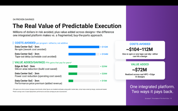
The $725 Million Chip Development: Why Execution Risk, Not IP Cost, Now Dictates Advanced-Node Survival

Source: https://semiwiki.com/artificial-intelligence/375867-the-725-million-chip-development-why-execution-risk-not-ip-cost-now-dictates-advanced-node-survival/ The philosophy of relying on a single, unified IP stack to lower your total cost of ownership is not a new concept invented just for the AI era. Semiconductor engineering teams have been weighing the trade-offs of piecemeal versus integrated intellectual property sourcing for

By Jeongwoo Heo
Generating Chip Subsystems Automatically: A New Answer to Manage Chip Design Complexity

semiconductor

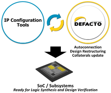
Generating Chip Subsystems Automatically: A New Answer to Manage Chip Design Complexity

Source: https://semiwiki.com/eda/defacto-technologies/375844-generating-chip-subsystems-automatically-a-new-answer-to-manage-chip-design-complexity/ By Defacto Staff Today’s chips are no longer just processors, they are entire systems. A System-on-Chip (SoC) brings together CPU clusters, accelerators, memories, interconnects and dozens of peripherals, often coming from many different teams and vendors. With AI, high-performance computing and IoT

By Jeongwoo Heo
Reimagining 3D IC Design: From Architecture to Signoff

semiconductor

Reimagining 3D IC Design: From Architecture to Signoff

Source: https://semiwiki.com/eda/siemens-eda/375653-reimagining-3d-ic-design-from-architecture-to-signoff/ By Keith Felton, Andras Vass-Varnai and Todd Burkholder, Siemens EDA The semiconductor industry is undergoing a fundamental transformation. Heterogeneous integration, the practice of combining multiple chiplets and specialized components into a single advanced packaging platform, has emerged as a powerful alternative to traditional

By Jeongwoo Heo
GSA Honors Sanjay Mehrotra as Memory Takes Center Stage in Computing

semiconductor

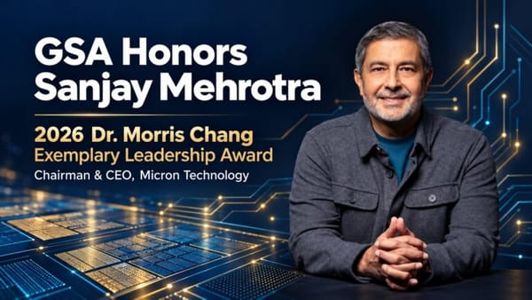
GSA Honors Sanjay Mehrotra as Memory Takes Center Stage in Computing

Source: https://semiwiki.com/events/375599-gsa-honors-sanjay-mehrotra-as-memory-takes-center-stage-in-computing/ The Global Semiconductor Alliance will present Micron Technology Chairman and CEO Sanjay Mehrotra with its 2026 Dr. Morris Chang Exemplary Leadership Award, recognizing a career that connects foundational flash memory innovation with the demands of modern computing. The presentation is scheduled for GSA’s

By Jeongwoo Heo
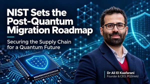
NIST Sets a Clearer Course for the Post-Quantum Security Transition

quantum

NIST Sets a Clearer Course for the Post-Quantum Security Transition

Source: https://semiwiki.com/security/pqshield/375585-nist-sets-a-clearer-course-for-the-post-quantum-security-transition/ NIST’s report, Transition to Post-Quantum Cryptography Standards, gives government agencies and technology suppliers a clearer framework for replacing cryptography vulnerable to future quantum computers. Its significance extends beyond selecting algorithms: it connects security priorities, application requirements and migration deadlines, helping organizations turn

By Jeongwoo Heo
CTO Interview with Ed Plowman of Imagination Technologies

semiconductor

CTO Interview with Ed Plowman of Imagination Technologies

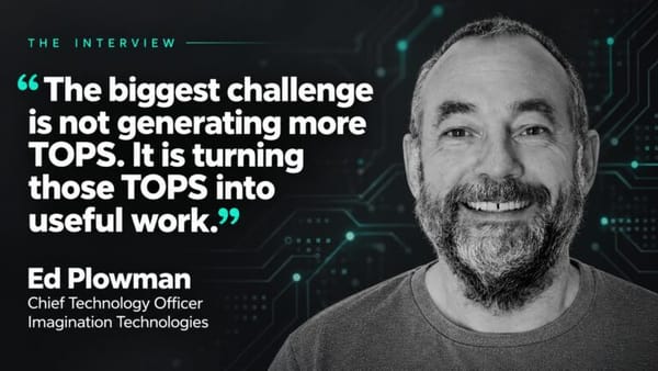
Source: https://semiwiki.com/ip/imagination-technologies/375737-cto-interview-with-ed-plowman-of-imagination-technologies/ Ed Plowman is Chief Technology Officer at Imagination Technologies, where he leads technology strategy, advanced architecture research and long-term innovation initiatives. He focuses on the convergence of graphics, compute and artificial intelligence, helping shape the next generation of efficient and adaptable computing platforms

By Jeongwoo Heo
Ceva’s next NeuPro generation opens new possibilities across AI

semiconductor

Ceva’s next NeuPro generation opens new possibilities across AI

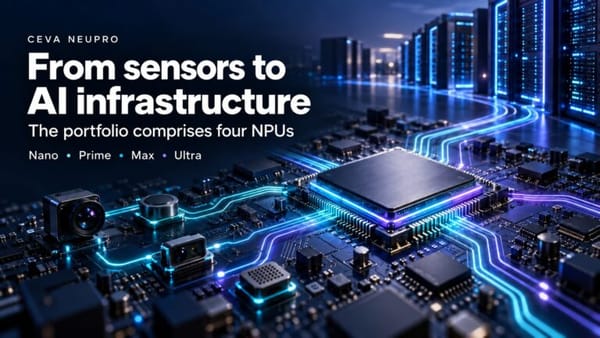
Source: https://semiwiki.com/ip/ceva/375670-cevas-next-neupro-generation-opens-new-possibilities-across-ai/ Ceva is broadening the possibilities for AI silicon with a new generation of its NeuPro neural processing unit portfolio, bringing a common architecture and unified software environment to applications spanning sensors, intelligent devices and cloud infrastructure. 세바(Ceva)는 센서, 지능형 기기, 클라우드

By Jeongwoo Heo