SemiWiki

Arteris FlexGen Opens Up Multi-Die Traffic Management for Non-Coherent Networks

semiconductor

Arteris FlexGen Opens Up Multi-Die Traffic Management for Non-Coherent Networks

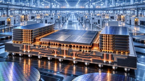
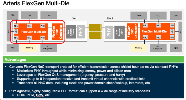
Source: https://semiwiki.com/ip/arteris/374391-arteris-flexgen-opens-up-multi-die-traffic-management-for-non-coherent-networks/ Last year I wrote about Arteris’ introduction of multi-die support for coherent NoCs. This is a very big deal because hyperscalers and OEMs are now building large systems that depend on multi-chiplet architectures and require efficient traffic management between chiplets, in one case
By Jeongwoo Heo
The Industry Challenge: AI Is Forcing Semiconductor Innovation Beyond the Chip

semiconductor

The Industry Challenge: AI Is Forcing Semiconductor Innovation Beyond the Chip

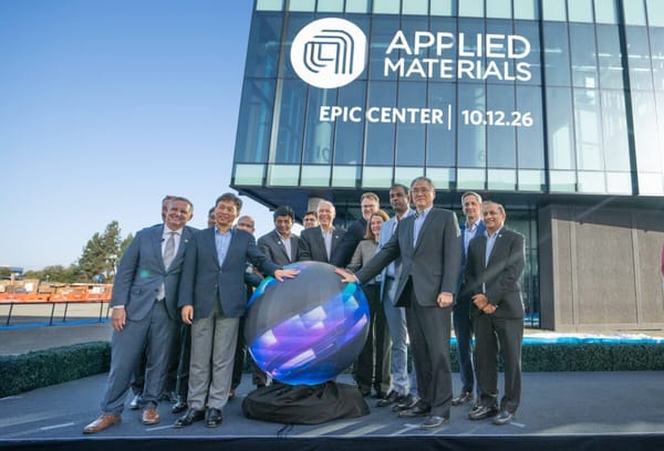
Source: https://semiwiki.com/semiconductor-manufacturers/applied-materials/375047-the-industry-challenge-ai-is-forcing-semiconductor-innovation-beyond-the-chip/ Applied Materials President and CEO Gary Dickerson with the EPIC Center founding partners on October 12, 2026, in Sunnyvale, CA. (Tomas Ovalle/AP Content Services for Applied Materials, Inc.) The bottlenecks are becoming interconnected 2026년 10월 12일 캘리포니아주 서니베일에서 EPIC 센터 창립 파트너들과

By Jeongwoo Heo
Who Gets to Move the Recipe? How Autonomous Agents Earn Decision Authority in the Fab

semiconductor

Who Gets to Move the Recipe? How Autonomous Agents Earn Decision Authority in the Fab

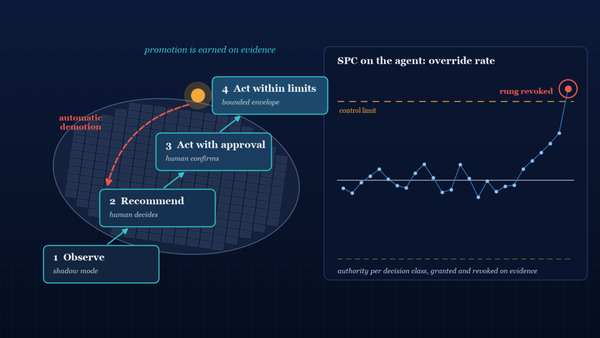
Source: https://semiwiki.com/eda/375060-who-gets-to-move-the-recipe-how-autonomous-agents-earn-decision-authority-in-the-fab/ by Ajay Kumar Govindaram 아제이 쿠마르 고빈다람(Ajay Kumar Govindaram) 글 There’s a question I’ve started asking at every agentic AI demo I sit through, and it has a clean answer in every fab on earth: who is allowed to change the

By Jeongwoo Heo
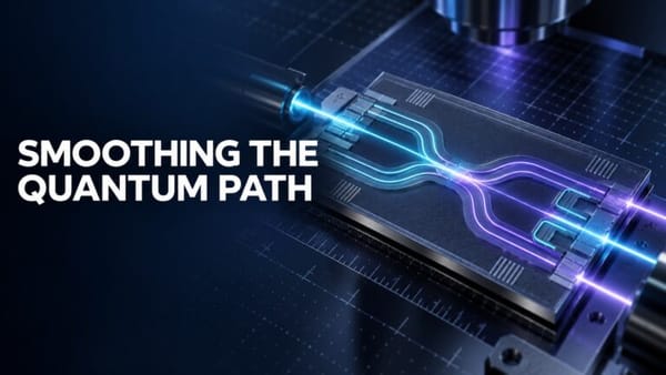
Smoothing the Quantum Path: ASML and Xanadu Target Photon Loss

semiconductor

Smoothing the Quantum Path: ASML and Xanadu Target Photon Loss

Source: https://semiwiki.com/lithography/373533-smoothing-the-quantum-path-asml-and-xanadu-target-photon-loss/ ASML’s decision to collaborate with Xanadu targets one of photonic quantum computing’s most unforgiving engineering constraints: photon loss. The companies will investigate advanced lithography processes for Xanadu’s photonic quantum hardware, focusing on whether tighter patterning control can suppress loss mechanisms and

By Jeongwoo Heo
Sir Arthur C. Clarke Deserves a Nobel Prize

semiconductor

Sir Arthur C. Clarke Deserves a Nobel Prize

Source: https://semiwiki.com/semiconductor-services/silicon-catalyst/375130-sir-arthur-c-clarke-deserves-a-nobel-prize/ By Richard Curtin 리차드 커틴(Richard Curtin) 글 Ever since the Silicon Catalyst 2023 Semiconductor Industry Forum (“Welcome to our AI Wonderland”) I’ve been convinced that the Nobel Prize committee needs to consider awarding a posthumous award to Sir Arthur. 실리콘 카탈리스트

By Jeongwoo Heo

semiconductor

Moving Beyond AI-Assisted Design – Agentrys Shows the Way with Agentic Loop Engineering

Source: https://semiwiki.com/eda/agentrys/375112-agentrys-shows-the-way-with-agentic-loop-engineering/ At Hot Chips 2026, OpenAI presented Jalapeño, an inference ASIC built with AI in the design loop. As reported from the session by ServeTheHome and Tom’s Hardware, OpenAI showed measured block-level wins over a human baseline — 56% on a BF16 multiply, alongside

By Jeongwoo Heo
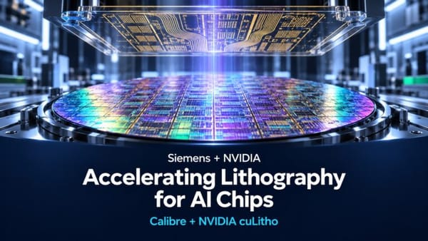
Siemens and NVIDIA Accelerate Lithography for Next-Generation AI Chips

semiconductor

Siemens and NVIDIA Accelerate Lithography for Next-Generation AI Chips

Source: https://semiwiki.com/eda/siemens-eda/374917-siemens-and-nvidia-accelerate-lithography-for-next-generation-ai-chips/ Siemens has announced advances in its collaboration with NVIDIA to accelerate computational lithography, addressing a demanding step in manufacturing advanced AI semiconductors. By integrating NVIDIA’s cuLitho library with Siemens Calibre manufacturing software, the companies aim to make sophisticated photomask optimization practical at

By Jeongwoo Heo
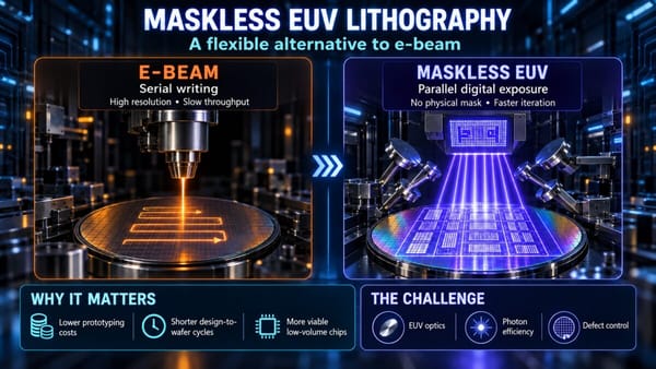
Maskless EUV Lithography: An Alternative to E-Beam

semiconductor

Maskless EUV Lithography: An Alternative to E-Beam

Source: https://semiwiki.com/lithography/373583-maskless-euv-lithography-an-alternative-to-e-beam/ Semiconductor manufacturing depends on lithography: the process of transferring tiny circuit patterns onto a silicon wafer. Conventional extreme-ultraviolet (EUV) lithography projects light with a wavelength of 13.5 nanometers through a reflective optical system, using a custom photomask to define each layer. It can

By Jeongwoo Heo
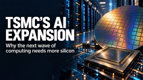
TSMC’s AI Expansion Signals a Broader Shift in Computing

semiconductor

TSMC’s AI Expansion Signals a Broader Shift in Computing

Source: https://semiwiki.com/semiconductor-manufacturers/tsmc/374950-tsmcs-ai-expansion-signals-a-broader-shift-in-computing/ TSMC is describing an artificial intelligence boom that reaches beyond accelerator chips into the wider computing infrastructure needed to support increasingly capable AI systems. On the recent investor call, Chairman and CEO Dr. C.C. Wei presents strong demand, persistent supply constraints and

By Jeongwoo Heo
Terafab’s Single Roof: Why Packaging, Not Lithography, Decides High Volume

semiconductor

Terafab’s Single Roof: Why Packaging, Not Lithography, Decides High Volume

Source: https://semiwiki.com/semiconductor-manufacturers/374838-terafabs-single-roof-why-packaging-not-lithography-decides-high-volume/ By Shaurya Seth Terafab is one of the most ambitious projects of the decade: $16.8 billion for phase one and up to $119 billion across four phases. A research fab in Austin iterates on process recipes, transistor designs, and packaging variants at a

By Jeongwoo Heo
Why Semiconductor AI Starts with Data, Not Algorithms

semiconductor

Why Semiconductor AI Starts with Data, Not Algorithms

Source: https://semiwiki.com/semiconductor-manufacturers/374900-why-semiconductor-ai-starts-with-data-not-algorithms/ The next gains from AI in semiconductors will come less from models and more from making fab and test data reliable, connected and tied to engineering decisions. 반도체 분야에서 AI가 가져올 다음 단계의 성장은 정교한 모델 그 자체보다는 팹(fab) 및 테스트 데이터를 신뢰할

By Jeongwoo Heo
Why AI Security Starts at the Chip Level

semiconductor

Why AI Security Starts at the Chip Level

Source: https://semiwiki.com/eda/synopsys/374743-why-ai-security-starts-at-the-chip-level/ Artificial intelligence is becoming part of the infrastructure that powers healthcare, transportation, finance, manufacturing, and everyday digital services. As these systems grow more capable, they also process more sensitive information and depend on increasingly complex hardware. The Synopsys white paper, “Securing AI at

By Jeongwoo Heo